
Front plate for plasma display panel and method for manufacturing the same, as well as plasma display panel

a plasma display panel and front plate technology, applied in the manufacture of electrode systems, cold cathode manufacturing, electric discharge tube/lamp manufacture, etc., can solve the problems of pdp quality degradation, and achieve the effects of suppressing the increase in manufacturing time and manufacturing cost, low viscosity, and low viscosity

Inactive Publication Date: 2011-09-15
PANASONIC CORP
View PDF1 Cites 2 Cited by
  • Summary
  • Abstract
  • Description
  • Claims
  • Application Information

AI Technical Summary

Benefits of technology

[0045]The front plate for PDP according to the present invention includes the large number of strip-shaped aid members formed in the region, where the dielectric material hardly flows, located between the adjacent terminal groups. Therefore, even in a case where a dielectric material to be used is low in viscosity, the aid member aids the flow of the dielectric material, so that the circumference of the dielectric layer can be made even.
[0046]Moreover, the PDP according to the present invention includes the front plate for PDP. In the PDP, therefore, the circumference of the dielectric layer can be made even although a dielectric material to be used is low in viscosity.
[0047]Further, the method for manufacturing the front plate for PDP according to the present invention allows simultaneous formation of the lead electrode and the aid member by exposure and development of the electrode material containing the photosensitive material. Therefore, no extra step is required for formation of the aid member, leading to suppression of increase in manufacturing time and manufacturing cost.

Problems solved by technology

The wavy circumference of the dielectric layer lowers a sealability of a seal member, leading to degradation in quality of a PDP.

Method used


Image

  • Front plate for plasma display panel and method for manufacturing the same, as well as plasma display panel
  • Front plate for plasma display panel and method for manufacturing the same, as well as plasma display panel
  • Front plate for plasma display panel and method for manufacturing the same, as well as plasma display panel

Examples


embodiments

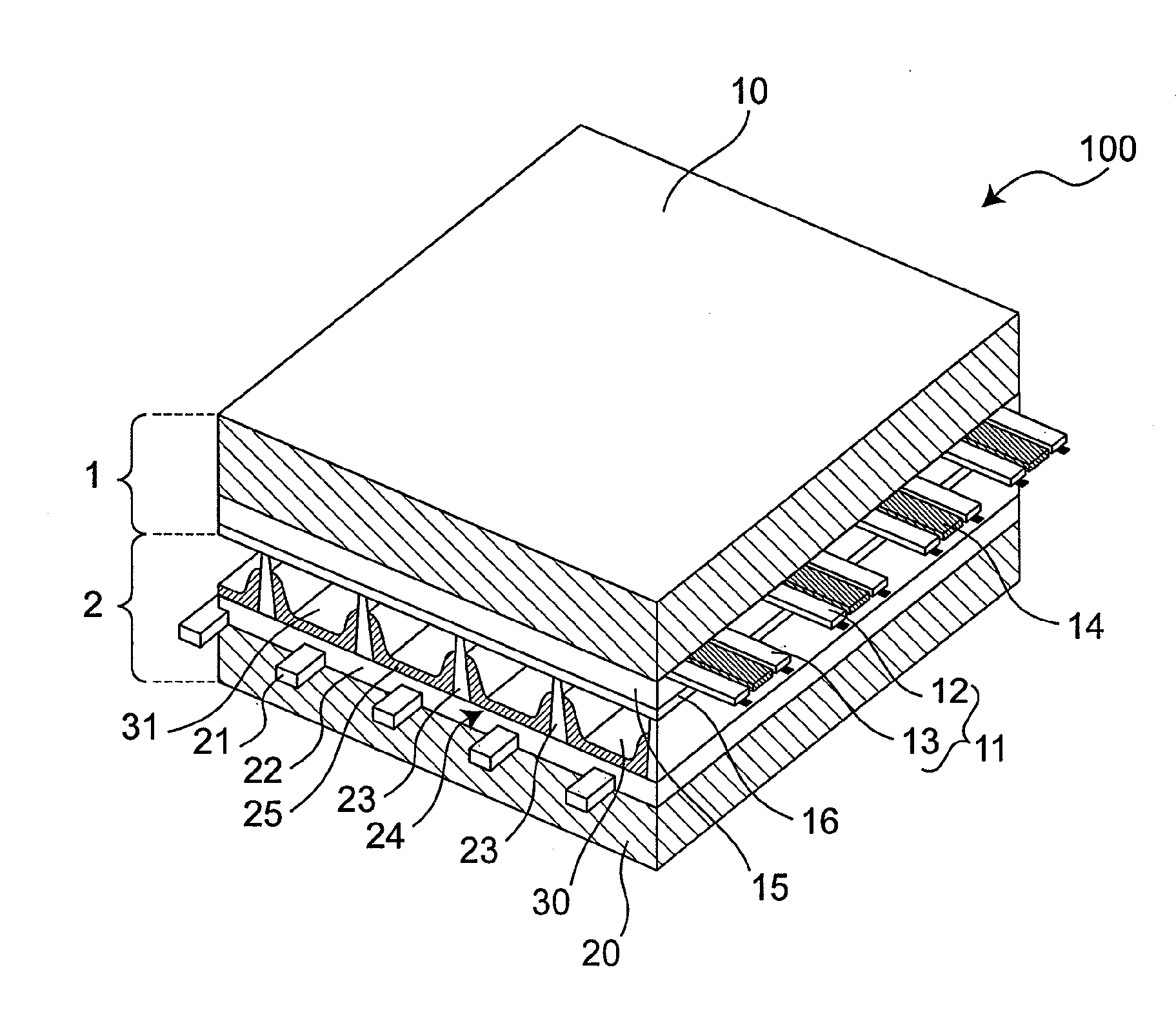
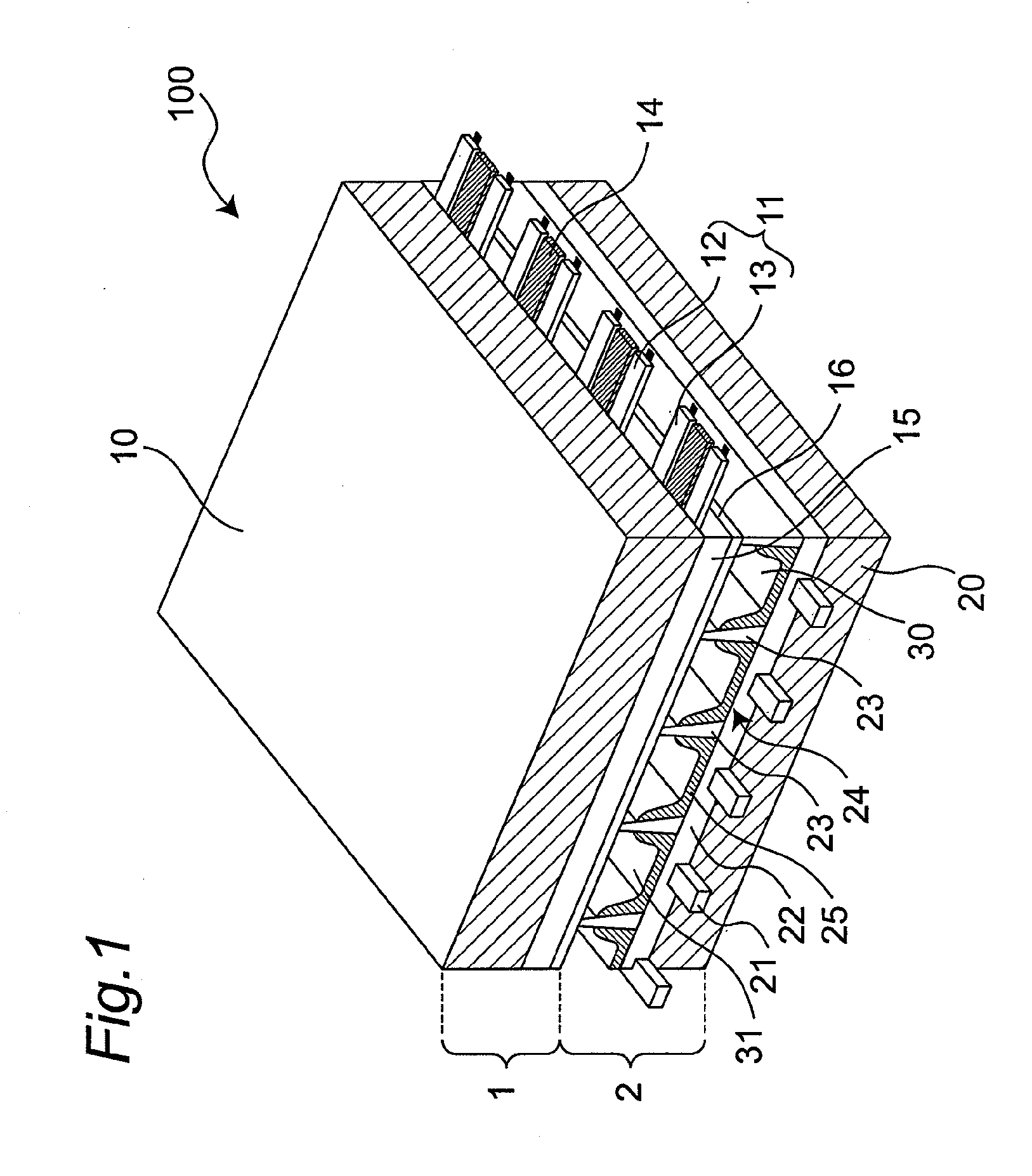
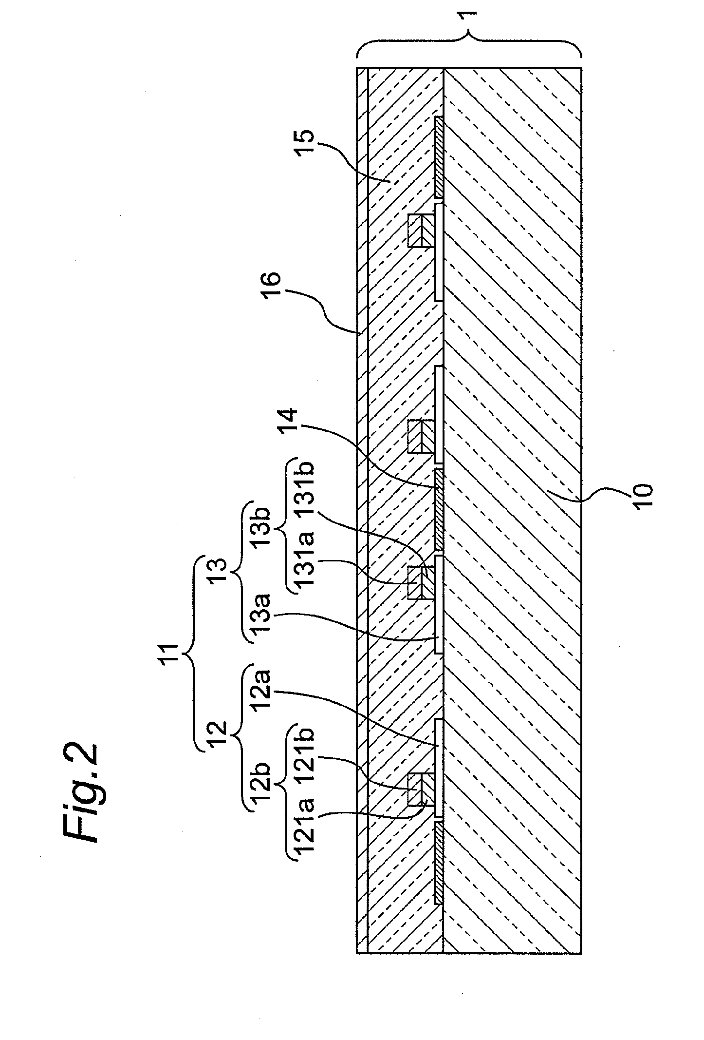
[0077]With reference to FIG. 1, description will be given of a basic configuration of a PDP 100 including a front plate for PDP according to one embodiment of the present invention (hereinafter, referred to as a front plate 1). FIG. 1 is a perspective view schematically showing a basic structure of the PDP 100 including the front plate 1 according to the embodiment of the present invention. The basic structure of the PDP 100 in this embodiment is similar to that of a typical PDP of an AC surface discharge type.

[0078]As shown in FIG. 1, the PDP 100 includes the front plate 1 and a back plate 2 arranged so as to face the front plate 1. Herein, an outer periphery between the front plate 1 and the back plate 2 is surrounded with a seal member 18 (see FIG. 3) such as glass frit. That is, the PDP 100 is sealed hermetically with the seal member 18, so that a discharge space 30 is formed inside the PDP 100. The discharge space 30 is filled with a discharge gas containing neon (Ne), xenon (X...


PUM


Abstract

In a front plate for PDP, which includes: a large number of display electrodes formed in stripes on a substrate; a plurality of terminal groups for connection with an external drive circuit, each terminal group being formed along an edge of the substrate, the edge being extended in a direction orthogonal to an extending direction of the display electrode; and a large number of lead electrodes extended from the display electrodes, respectively, in a non-image display region on the substrate to gather toward any one of the terminal groups without intersecting each other, the lead electrodes being connected to corresponding terminals in the relevant terminal group, respectively, further, a large number of strip-shaped aid members for aiding formation of a dielectric layer are formed in a region located between the adjacent terminal groups. Thus, it is possible to make a circumference of a dielectric layer even although a dielectric material to be used is low in viscosity.

Description

TECHNICAL FIELD[0001]The present invention relates to a plasma display panel for use in an image display device and the like. More specifically, the present invention relates to a configuration and a manufacturing method of a non-image display region on an outer periphery of a front plate of the plasma display panel.BACKGROUND ART[0002]A plasma display panel (hereinafter, referred to as a PDP) allows realization of a high degree of definition and a large screen, and therefore is for use in a large television set having a screen size of, for example, 65 inches or more. Recently, such a PDP has been applied increasingly to a high-definition television set having scanning lines the number of which is more than twice as large as those of a conventionally known television set adopting an NTSC system, and further reduction in cost thereof has been demanded.[0003]A PDP basically includes a front plate and a back plate. The front plate typically includes a front substrate, a large number of...

Claims


Application Information

Patent Timeline
Patent Type & Authority Applications(United States)
IPC IPC(8): H01J17/49H01J9/24H01J11/12H01J11/32H01J11/46
CPCH01J9/185H01J11/12H01J2211/46H01J11/46H01J2211/323H01J11/32
Inventor TSUCHIDA, SHUZO
Owner PANASONIC CORP
Learn More