ESD protection device and method for manufacturing the same

a protection device and electrostatic discharge technology, applied in the direction of shielding materials, semiconductor/solid-state device details, spark plugs, etc., can solve the problems of difficult to achieve the responsivity desired by esd, limited adjustment amount by the size of the product, damage or malfunction of electronic devices, etc., to prevent degradation of discharge characteristics caused by repetitive discharges, and easy to adjust and stabiliz

Active Publication Date: 2011-09-15
MURATA MFG CO LTD
View PDF3 Cites 35 Cited by
  • Summary
  • Abstract
  • Description
  • Claims
  • Application Information

AI Technical Summary

Benefits of technology

[0078]In this case, the contact between particles of the conductive material powder of the supporting electrode portion can be easily prevented.
[0079]According to a preferred embodiment of the present invention, the ESD characteristics of an ESD device are easily adjusted and stabilized.
[0080]According to another preferred embodiment of the present invention, the ESD characteristics of an ESD device are easily adjusted and stabilized and thus the degradation of discharge characteristics caused by repetitive discharges are prevented.
[0081]According to yet another preferred embodiment of the present invention, the discharge starting voltage can be set with high precision and an ESD protection device having high reliability can be manufactured.

Problems solved by technology

ESD causes damage or malfunctioning of electronic devices.
An excessively high voltage, for example, generated by static electricity through an antenna of a cellular phone causes discharge between the discharge electrodes of the ESD protection device, which leads the static electricity to the ground.
Furthermore, although the responsivity to ESD needs to be adjusted using an area of the region sandwiched between discharge electrodes facing each other, the amount of adjustment is limited by the size of the product or other factors.
Therefore, it may be difficult to achieve a desired responsivity to ESD.
However, with such a structure, since the conductive material is scattered due to an impact caused during discharge and thus the distribution density is decreased, the discharge voltage is gradually increased each time discharge is performed.
Firstly, a discharge starting voltage is primarily set by adjusting the distance between discharge electrodes. However, the distance between discharge electrodes is varied because of variations that occur during production and a difference in shrinkage behavior between a ceramic multilayer substrate and discharge electrodes during firing. Consequently, the discharge starting voltage of an ESD protection device varies. Therefore, the discharge starting voltage cannot be set with high precision.
Secondly, discharge electrodes in a cavity may be detached from a ceramic multilayer substrate because of a decrease in the hermeticity of the cavity or a difference in a coefficient of thermal expansion (may be referred to as “thermal expansivity”) between a base layer of the ceramic multilayer substrate and the discharge electrodes. In such a case, the device becomes unusable as an ESD protection device, or the discharge starting voltage is changed and, thus, the reliability of the ESD protection device is degraded.

Method used


Image

  • ESD protection device and method for manufacturing the same
  • ESD protection device and method for manufacturing the same
  • ESD protection device and method for manufacturing the same

Examples


example 1-1

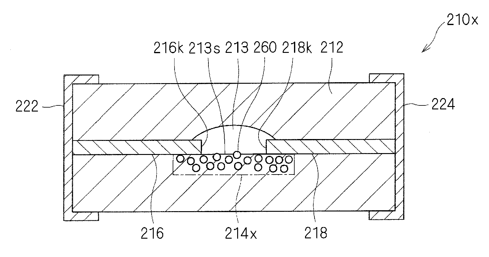
[0122]An ESD protection device 10 of an Example 1-1 of a preferred embodiment of the present invention will be described with reference to FIGS. 1 to 6.

[0123]FIG. 1 is a sectional view of an ESD protection device 10. As shown in FIG. 1, the ESD protection device 10 preferably includes a cavity 13 provided in a substrate body 12 of a ceramic substrate. A pair of discharge electrodes 16 and 18 are arranged such that the respective edges 16k and 18k are exposed in the cavity 13. The discharge electrodes 16 and 18 are arranged so that the edges 16k and 18k face each other with a space provided therebetween. The discharge electrodes 16 and 18 extend to the peripheral surface of the substrate body 12 and are respectively connected to external electrodes 22 and 24 provided on the surface of the substrate body 12. The external electrodes 22 and 24 are used to connect the ESD protection device 10 to another device.

[0124]As schematically shown in FIG. 1, a plurality of supporting electrode pa...

modification 1-1

[0185]A Modification 1-1 of a preferred embodiment of the present invention will be described with reference to FIGS. 7 and 8.

[0186]Modification 1-1 is a modification of Example 1-1. Hereinafter, the same elements and components as those in Example 1-1 are designated by the same reference numerals, and the differences between Example 1-1 and Modification 1-1 will be primarily described.

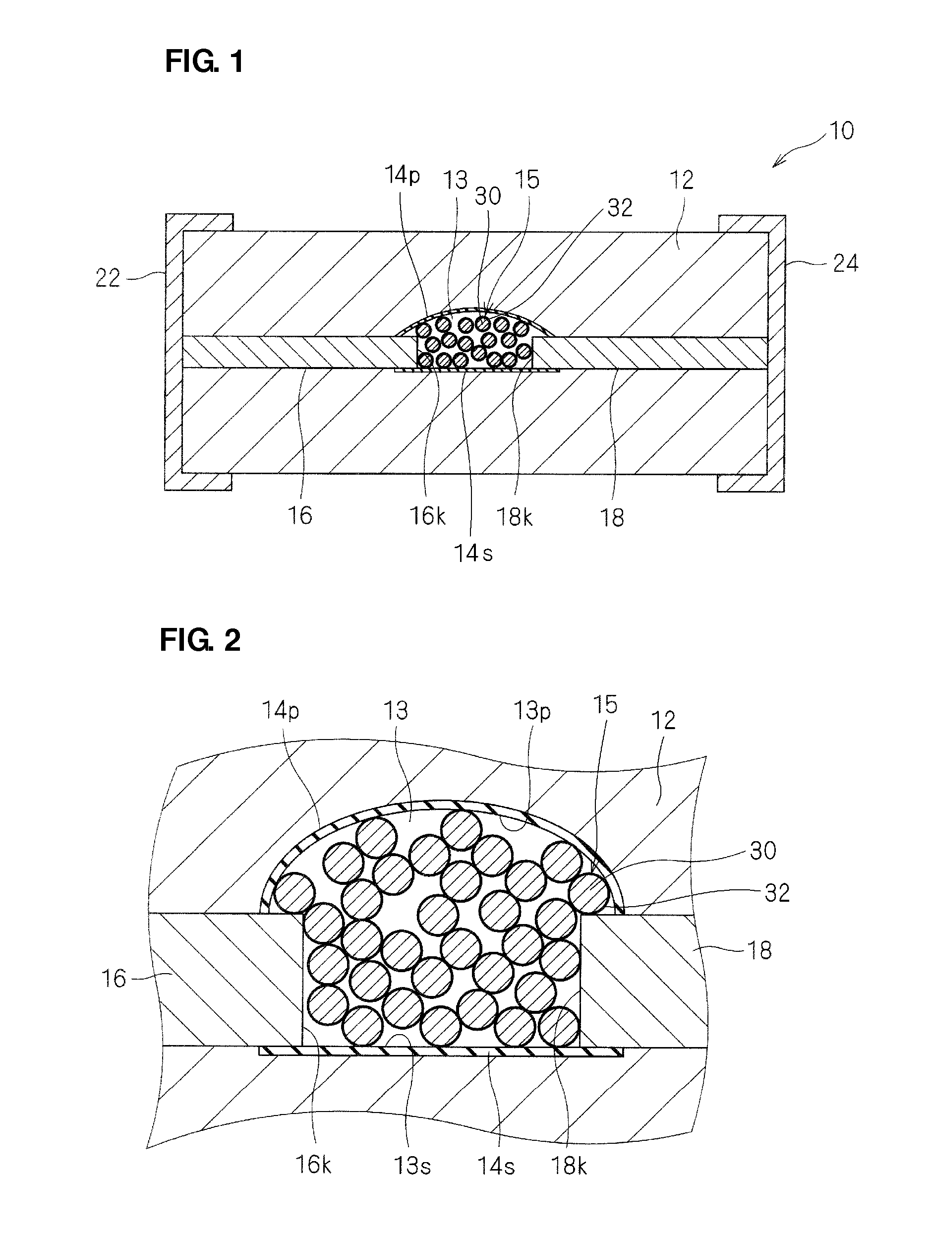
[0187]FIG. 7 is a sectional view of an ESD protection device 10a of Modification 1-1. FIG. 8 is an enlarged sectional view of a principal portion that shows a cavity 13a of the ESD protection device 10a of Modification 1-1.

[0188]As shown in FIGS. 7 and 8, in the ESD protection device 10a of Modification 1-1, the height of the cavity 13a including a supporting electrode material dispersed therein is substantially equal to the thickness of the discharge electrodes 16 and 18. In other words, a sealing member 14q that defines a top surface 13q of the cavity 13a extends so as to have a planar shape.

[0189]C...

example 1-2

[0190]An ESD protection device of an Example 1-2 of a preferred embodiment of the present invention will be described with reference to FIGS. 9 and 10.

[0191]The ESD protection device of Example 1-2 has substantially the same configuration as that of the ESD protection device 10 of Example 1-1. Hereinafter, the same elements and components as those in Example 1-1 are designated by the same reference numerals, and the differences between Example 1-1 and Example 1-2 will be primarily described.

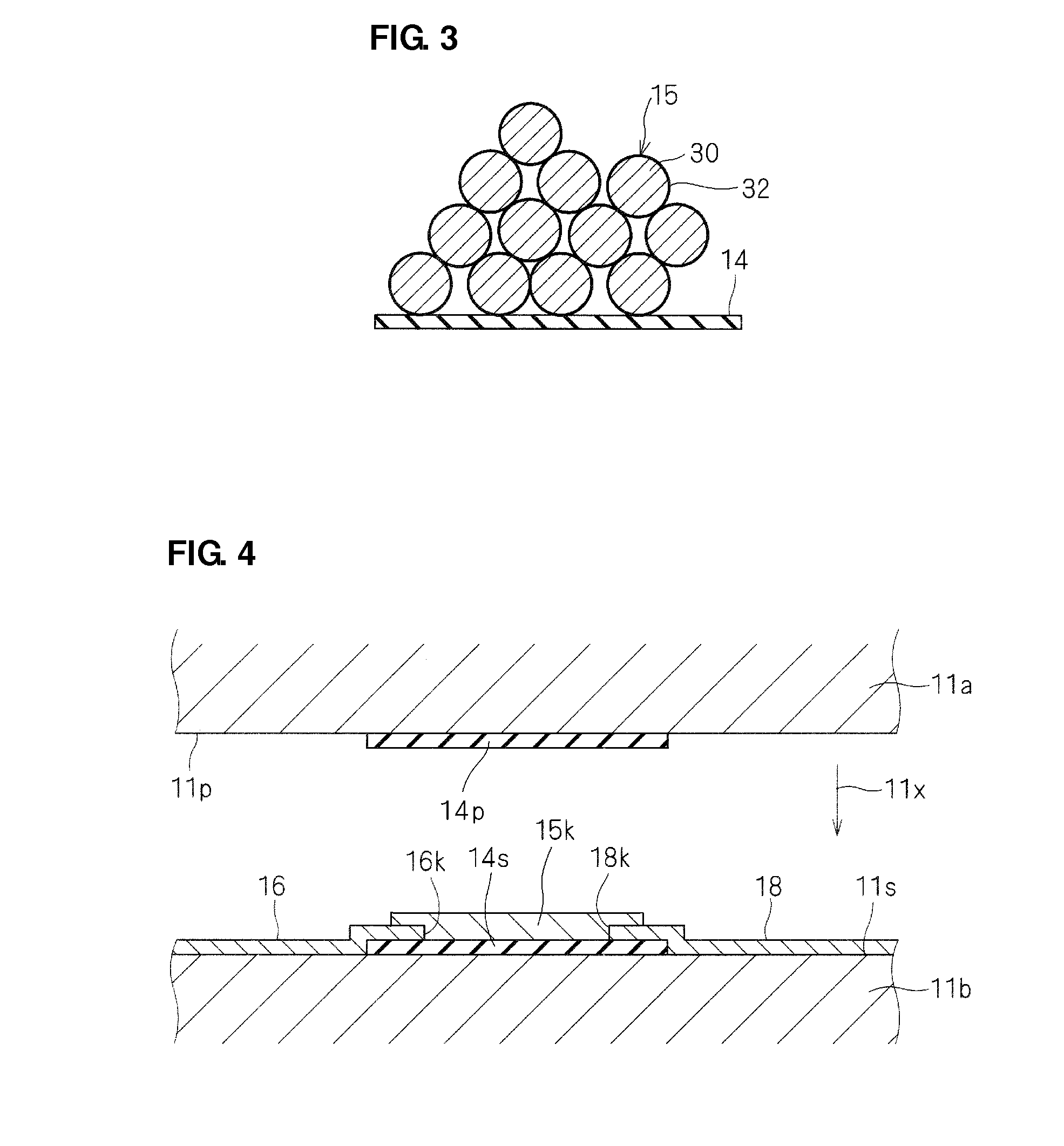
[0192]FIG. 9 is an enlarged sectional view of a principal portion of a cavity 13. As shown in FIG. 9, the ESD protection device of Example 1-2 is different from the ESD protection device 10 of Example 1-1 in that, in addition to the supporting electrode particles 15 including a supporting electrode material, insulating particles 15s are dispersed in the cavity 13. That is, the supporting electrode includes a mixture of the supporting electrode particles 15 and the insulating particles 15s. The pa...


PUM

PropertyMeasurementUnit
thicknessaaaaaaaaaa
particle sizeaaaaaaaaaa

Abstract

An ESD protection device is manufactured such that its ESD characteristics are easily adjusted and stabilized. The ESD protection device includes an insulating substrate, a cavity provided in the insulating substrate, at least one pair of discharge electrodes each including a portion exposed in the cavity, the exposed portions being arranged to face each other, and external electrodes provided on a surface of the insulating substrate and connected to the at least one pair of discharge electrodes. A particulate supporting electrode material having conductivity is dispersed between the exposed portions of the at least one pair of discharge electrodes in the cavity

Description

BACKGROUND OF THE INVENTION[0001]1. Field of the Invention[0002]The present invention relates to an electrostatic discharge (ESD) protection device and a method for manufacturing the ESD protection device, and particularly to an ESD protection device having improved ESD characteristics, such as discharge starting voltage, and reliability in which discharge electrodes are disposed in a cavity of an insulating substrate so as to face each other.[0003]2. Description of the Related Art[0004]ESD is a phenomenon in which strong discharge is generated when a charged conductive body (e.g., human body) comes into contact with or comes sufficiently close to another conductive body (e.g., electronic device). ESD causes damage or malfunctioning of electronic devices. To prevent this, an excessively high voltage generated during discharge must be prevented from being applied to circuits of the electronic devices. ESD protection devices, which are also called surge absorbers, are used for such an...

Claims


Application Information

Patent Timeline
Patent Type & Authority Applications(United States)
IPC IPC(8): H02H9/00H05K13/00
CPCH01T4/12Y10T29/49002H02H9/044H01T21/00H01B1/20H01T4/10H02H9/04H05K9/0067H05K9/0069H05K9/0079
Inventor ADACHI, JUNURAKAWA, JUNYAMAMOTO, ISSEI
Owner MURATA MFG CO LTD
Why Eureka
Try Eureka