
Semiconductor power device and manufacturing method thereof

a technology of semiconductors and power devices, applied in semiconductor devices, electrical devices, transistors, etc., can solve the problems of increased complexity and processing time of manufacturing processes, low yield, higher manufacturing costs, etc., and achieve the effect of simplifying processing steps, reducing the number of masks, and improving yield

Active Publication Date: 2011-09-29
SINOPOWER SEMICON
View PDF10 Cites 26 Cited by
  • Summary
  • Abstract
  • Description
  • Claims
  • Application Information

AI Technical Summary

Benefits of technology

[0010]The manufacturing method of the present invention only needs three or four masks to form a semiconductor power device having a shield electrode. Also, the semiconductor power device can combine with a new termination structure of the present invention. Therefore, the semiconductor power device and the manufacturing method thereof of the present invention can reduce the number of the masks to simplify the processing steps, improve the yield, and decrease the manufacturing cost.

Problems solved by technology

Thus, the complexity and the processing time of the manufacturing process are increased due to the larger number of the masks, and this undesirably results in a higher manufacturing cost and a low yield.

Method used


Image

  • Semiconductor power device and manufacturing method thereof
  • Semiconductor power device and manufacturing method thereof
  • Semiconductor power device and manufacturing method thereof

Examples


Embodiment Construction

[0018]In the following specifications and claims, certain terms are used throughout the description and following claims to refer to particular components. As one skilled in the art will appreciate, electronic equipment manufacturers may refer to a component by different names. This document does not intend to distinguish between components that differ in name but not function. In the following description and in the claims, the terms “include” and “comprise” are used in an open-ended fashion, and thus should be interpreted to mean “include, but not limited to”. For the convenience of comparison between each of the embodiments of the present invention, identical elements are denoted by identical numerals. In addition, it should be noted that the diagrams are for explanations and are not drawn as original sizes or to scale.

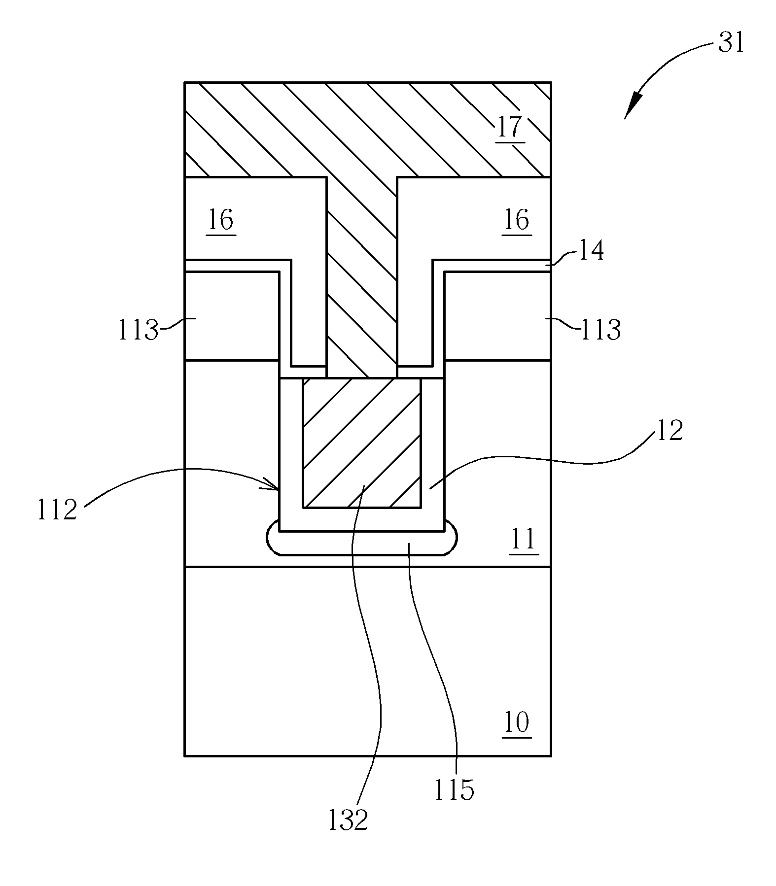
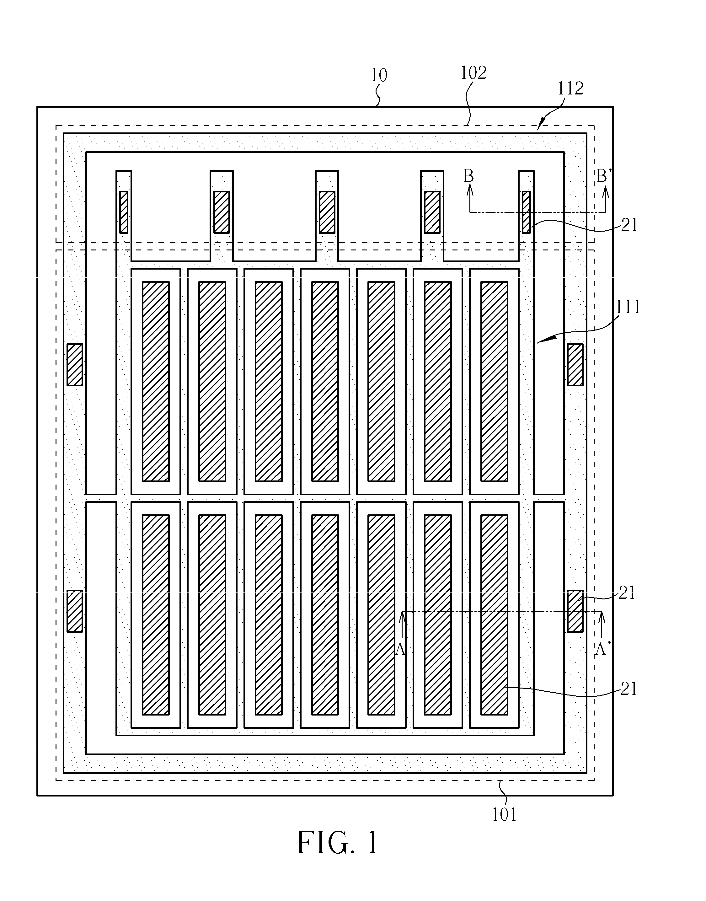
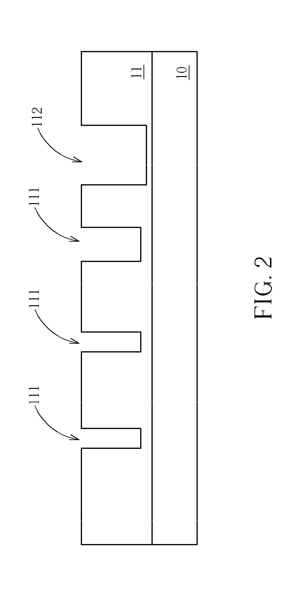
[0019]Please refer to FIG. 1. FIG. 1 is a schematic diagram illustrating a layout of a semiconductor power device according to a first preferred embodiment of the ...


PUM


Abstract

A semiconductor power device is provided, and a manufacturing method thereof includes the following steps. First, a substrate is provided, and an epitaxial layer is formed on the substrate. Then, at least a first trench and at least a second trench are formed in the epitaxial layer. Subsequently, a shield electrode and a termination electrode are respectively formed in the first trench and the second trench, and upper sidewalls of the first trench and the second trench are exposed. Following that, a gate dielectric layer is covered. Then, a second conductive layer is deposited to fill up the first trench and partially fill in the second trench. Subsequently, the second conductive layer is etched to remove the second conductive layer in the second trench and form a gate electrode in the first trench. Accordingly, the present invention can reduce the number of masks.

Description

BACKGROUND OF THE INVENTION[0001]1. Field of the Invention[0002]The present invention relates to a semiconductor power device and a manufacturing method thereof, and more particularly, to a semiconductor power device and a manufacturing method thereof to reduce the number of masks in the manufacturing process.[0003]2. Description of the Prior Art[0004]A trench metal-oxide-semiconductor field effect transistor (Trench MOSFET) is a common semiconductor power device. In the trench metal-oxide-semiconductor field effect transistor, a gate electrode is disposed in a trench of a substrate, and a source electrode and a drain electrode are respectively disposed at an upper side and a lower side of the gate electrode. A channel is vertically formed between the source electrode and the drain electrode. Accordingly, some advantages are provided by this structure, such as a high voltage-withstand ability, a low on-resistance, and a larger current. As a result, the trench metal-oxide-semiconduct...

Claims


Application Information

Patent Timeline
Patent Type & Authority Applications(United States)
IPC IPC(8): H01L29/78H01L21/336
CPCH01L29/0696H01L29/0865H01L29/0878H01L29/407H01L29/41766H01L29/7813H01L29/4238H01L29/66727H01L29/66734H01L29/7811H01L29/4236
Inventor TAI, SUNG-SHAN
Owner SINOPOWER SEMICON
Features
  • Generate Ideas
  • Intellectual Property
  • Life Sciences
  • Materials
  • Tech Scout
  • Unparalleled Data Quality
  • Higher Quality Content
  • 60% Fewer Hallucinations
Learn More