

Debonding equipment and methods for debonding temporary bonded wafers
a technology of temporary bonding and equipment, which is applied in the direction of electrical equipment, pile separation, and soldering auxiliaries, etc., can solve the problems of thinned wafers breaking, increasing the difficulty of mechanical holding of wafers, and increasing the difficulty of maintaining planarity and integrity
- Summary
- Abstract
- Description
- Claims
- Application Information
AI Technical Summary
Benefits of technology
Problems solved by technology
Method used
Image

Examples
Embodiment Construction
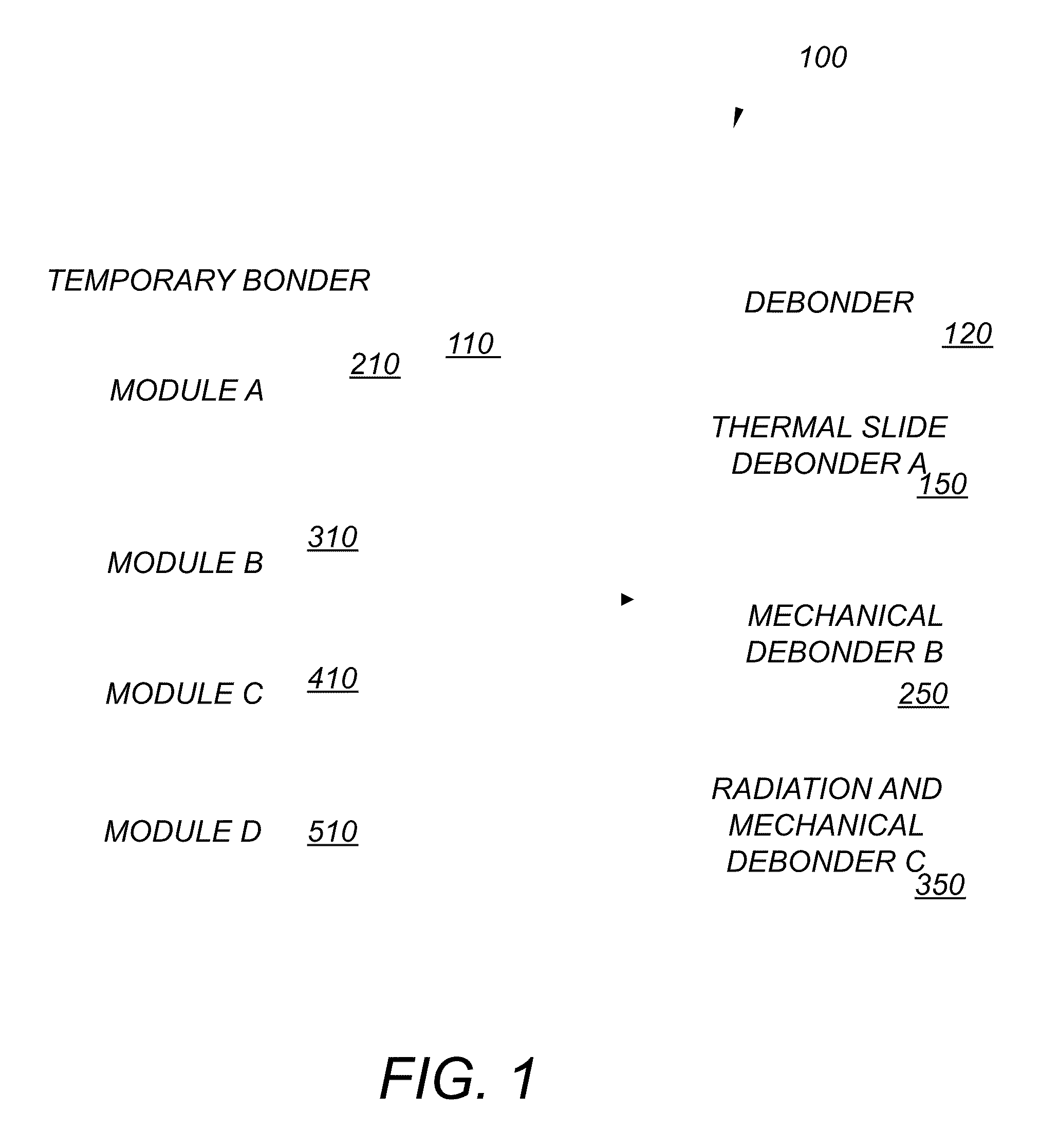
[0058]Referring to FIG. 1, an improved apparatus for temporary wafer bonding 100 includes a temporary bonder cluster 110 and a debonder cluster 120. The temporary bonder cluster 110 includes temporary bonder module A, module B, module C, and module D, 210, 310, 410 and 510 respectively. Debonder cluster 120 includes a thermal slide debonder A 150, a mechanical debonder B 250 and a radiation / mechanical debonder C 350. Bonder cluster 110 facilitates the temporary bonding processes A, B, C, and D, 60a, 70a, 80a and 90a, shown in FIG. 1A, FIG. 2A, FIG. 3A, and FIG. 4, respectively, among others. Debonder cluster 120 facilitates the debonding processes A, B and C, 60b, 70b, 80b, shown in FIG. 1A, FIG. 2A and FIG. 3A, respectively.
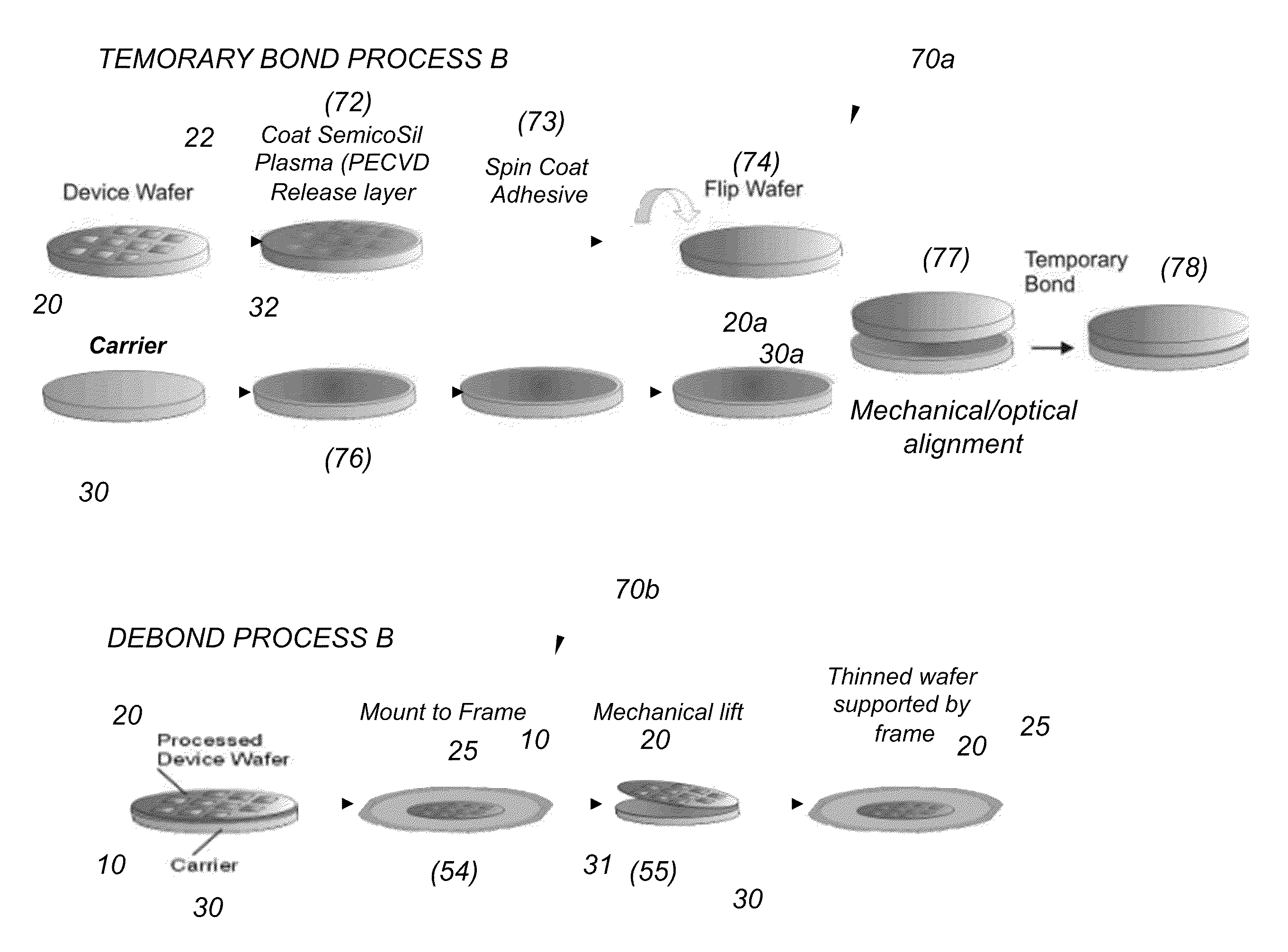
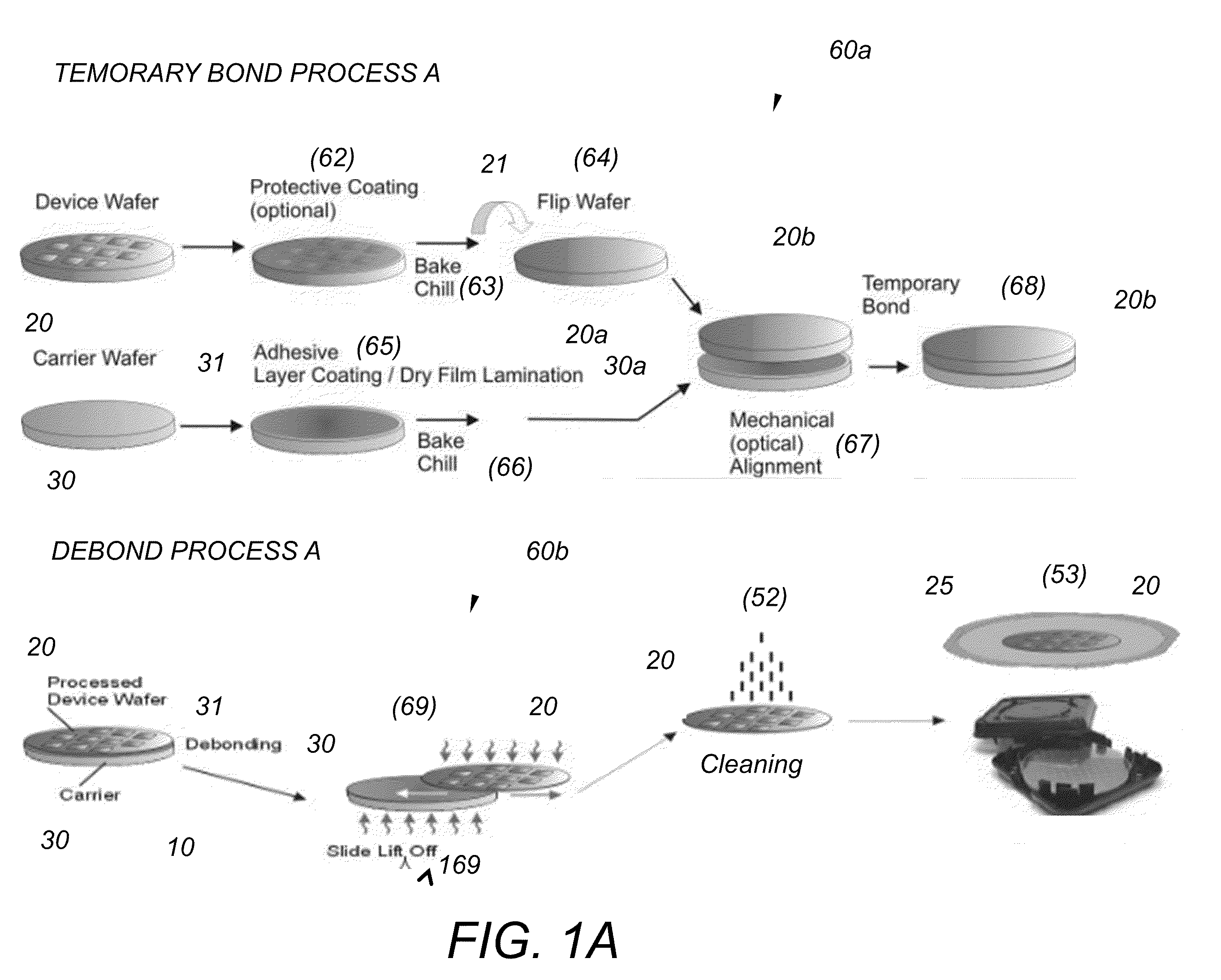
[0059]Referring to FIG. 1A, temporary bond process A 60a includes the following steps. First, device wafer 20 is coated with a protective coating 21 (62), the coating is then baked and chilled (63) and then the wafer is flipped (64). A carrier wafer 30 is coate...
PUM
| Property | Measurement | Unit |
|---|---|---|
| Pressure | aaaaa | aaaaa |
| Adhesivity | aaaaa | aaaaa |
Abstract
Description
Claims
Application Information