Processing method and storage medium

a processing method and storage medium technology, applied in the direction of basic electric elements, semiconductor/solid-state device manufacturing, electric apparatus, etc., can solve the problem that the recovery effect of the silylation process may not be improved as much as expected, and achieve the effect of shortening the processing time, enhancing the processing characteristics and throughput, and reducing the internal pressure of the chamber

Inactive Publication Date: 2008-08-14
TOKYO ELECTRON LTD
View PDF3 Cites 7 Cited by
  • Summary
  • Abstract
  • Description
  • Claims
  • Application Information

AI Technical Summary

Benefits of technology

[0017]In accordance with the present invention, it is possible to obtain a desired effect even with a lower pressure and a shorter processing time than those are in a conventional case as long as the internal pressure of the chamber by the supply of the gas having the Si—CH3 bond and the gas supply time are set to be within ranges where the silylation process can be performed, while the internal pressure of the chamber is decreased to reach an eligible pressure level where the wafer can be unloaded after the internal pressure of the chamber is increased up to the target pressure by the supply of the gas. Therefore, both processing characteristics and throughput can be enhanced. Specifically, after the chamber internal pressure reaches the preset pressure by the supply of the gas having the Si—CH3 bond, the internal pressure of the chamber is decreased without being maintained at the preset pressure. Accordingly, it is possible to maintain good processing characteristics by the short processing time.

Problems solved by technology

The present inventors have found that when performing the silylation process, even if an internal pressure of a processing chamber by supply of the gas having a Si—CH3 bond is set high and a maintenance time at a reached temperature is long, a recovery effect of the silylation process may not be improved as much as expected.

Method used


Image

  • Processing method and storage medium
  • Processing method and storage medium
  • Processing method and storage medium

Examples


Embodiment Construction

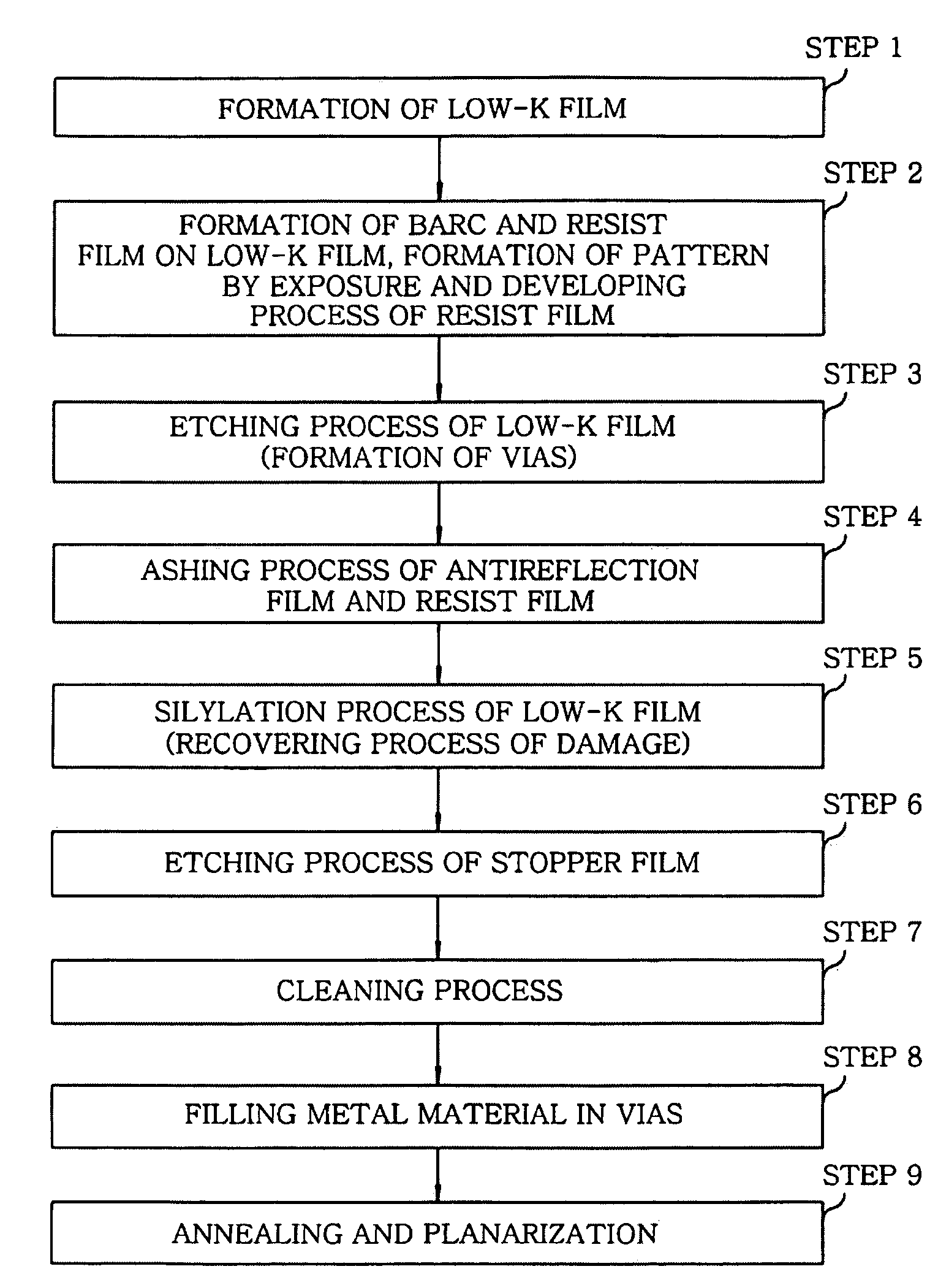
[0027]Hereinafter, an embodiment of the present invention will be described in detail with reference to the accompanying drawings, which form a part hereof. The embodiment will be explained for an exemplary case of applying a processing method in accordance with the present invention to the manufacture of a semiconductor device using a single or dual damascene method.

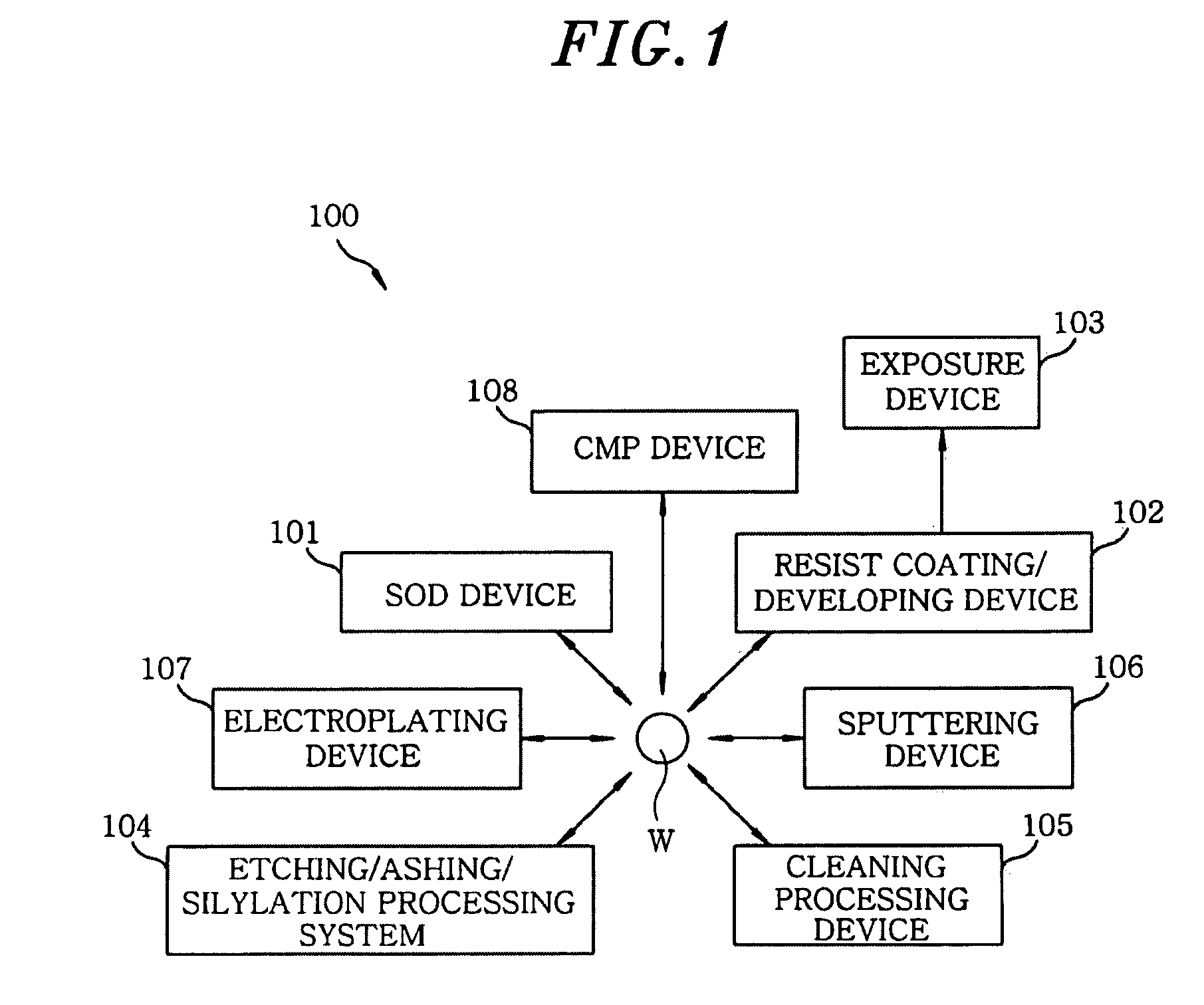
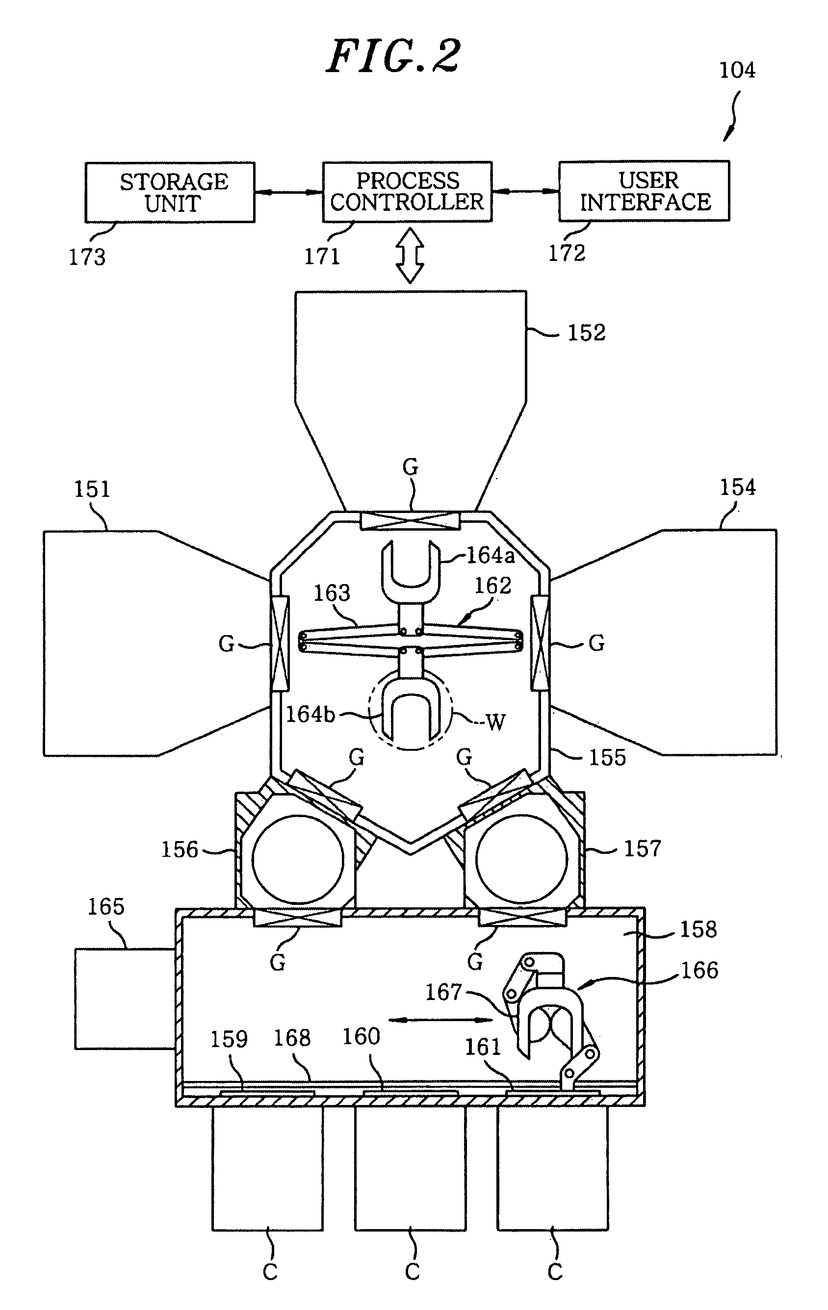
[0028]FIG. 1 is an explanatory diagram showing a schematic configuration of a semiconductor device manufacturing system 100 using a silylation processing unit which realizes the processing method of the present invention. The semiconductor device manufacturing system 100 includes an SOD (Spin On Dielectric) device 101; a resist coating / developing device 102; an exposure device 103; an etching / ashing / silylation processing system 104 for performing an etching process, a dry ashing process, and a silylation process; a cleaning processing device 105, a sputtering device 106 which is one of PVD (Physical Vapor Deposition) ap...


PUM


Abstract

A processing method includes a gas having a Si—CH3 bond supplied into a processing chamber after a target substrate to be processed is loaded into the processing chamber; and a silylation process performed on the target substrate. The internal pressure of the chamber by the supply of the gas having the Si—CH3 bond and the gas supply time are set to be within ranges where the silylation process can be performed while the internal pressure of the chamber is decreased to reach an eligible pressure level where the wafer can be unloaded after the internal pressure of the chamber is increased up to a preset pressure by the supply of the gas.

Description

FIELD OF THE INVENTION [0001]The present invention relates to a processing method for performing a silylation process on a semiconductor device formed by using, for example, a single damascene or dual damascene method; and a storage medium storing therein a program used to execute the processing method.BACKGROUND OF THE INVENTION [0002]In a manufacturing process of a semiconductor device, a dual damascene method has been widely used to form wiring trenches or connection holes (see, for example, Japanese Patent Laid-open Application No. 2002-83869).[0003]Meanwhile, with the miniaturization of the semiconductor device, a parasitic capacitance of an interlayer dielectric becomes an important factor for improving a wiring performance, and a low dielectric constant material (low-k material) is used to form the interlayer dielectric. As the low-k material for forming the interlayer dielectric, a material having an alkyl group such as a methyl group as an end group is generally utilized.[0...

Claims


Application Information

Patent Timeline
Patent Type & Authority Applications(United States)
IPC IPC(8): H01L21/469
CPCH01L21/3105H01L21/31058H01L21/76835H01L21/76814H01L21/76826H01L21/76802
Inventor KUBOTA, KAZUHIROHOSHI, NAOTSUGUCHIBA, YUKIASAKO, RYUICHI
Owner TOKYO ELECTRON LTD
Why Eureka
Try Eureka