Method for detecting variance in semiconductor processes

Active Publication Date: 2011-10-20
MICRON TECH INC
View PDF2 Cites 12 Cited by
  • Summary
  • Abstract
  • Description
  • Claims
  • Application Information

AI Technical Summary

Benefits of technology

[0010]The essential objective of the present invention is to provide a method for detecting variation in semiconductor processes, by using correlation analysis to locate the cau

Problems solved by technology

Therefore, how to enhance the yield has become one momentous issue of attention to which most semiconductor manufacturers closely and prudently pay.
However, in terms of the correlation of the machine, the aforementioned patent can only be applied in detection single semiconductor or single process step, and cannot

Method used


Image

  • Method for detecting variance in semiconductor processes
  • Method for detecting variance in semiconductor processes
  • Method for detecting variance in semiconductor processes

Examples


Embodiment Construction

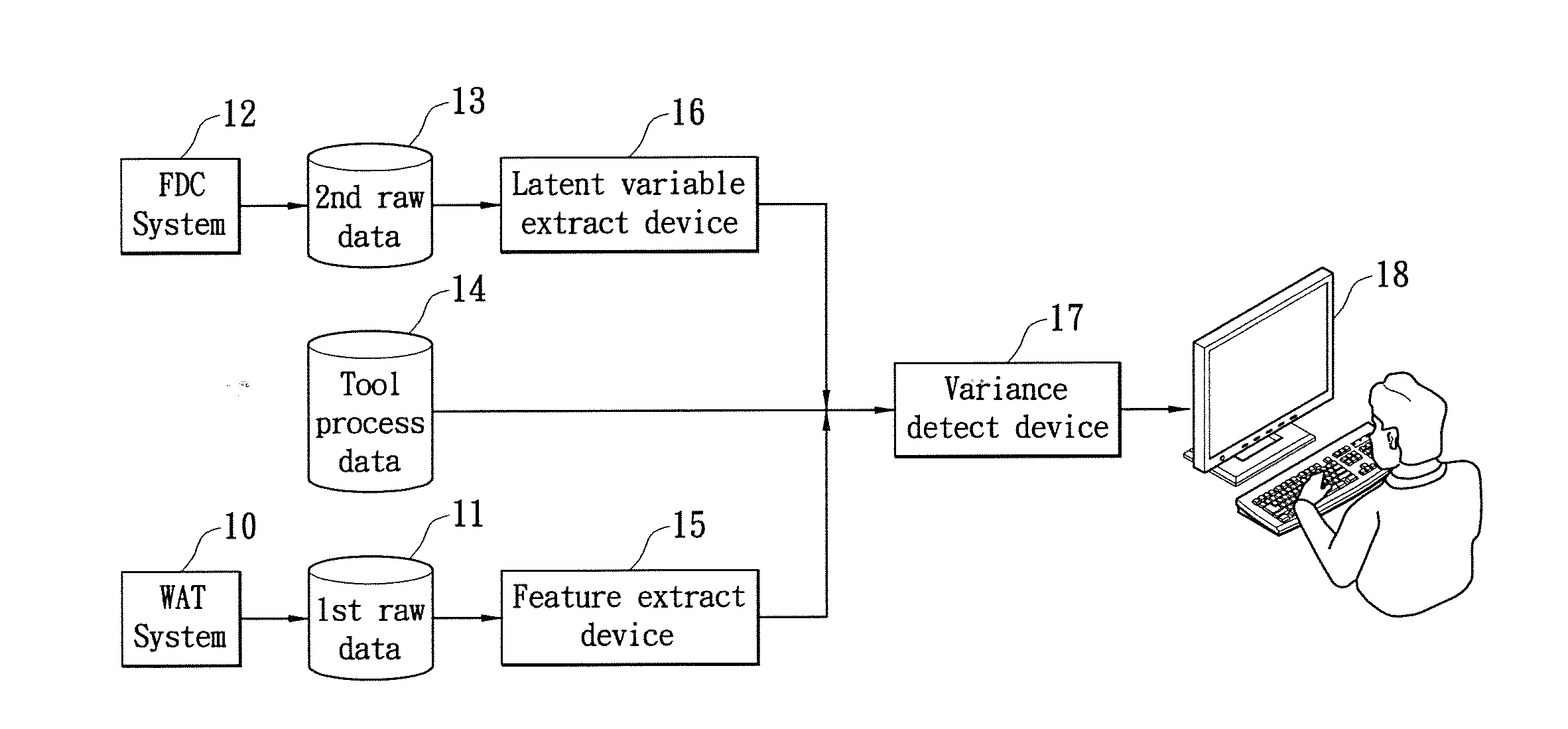
[0030]Refer now to FIG. 3, wherein the present invention proposes a method for detecting variation in semiconductor processes, which method for detecting variation in semiconductor processes comprises the following steps:

[0031]S100: collecting a plurality of tool process data, a plurality of first raw data and a plurality of second raw data, and pre-processing said first raw data and said second raw data;

[0032]S102: using a first statistic analysis method to process said first raw data in order to generate a plurality of correlation data;

[0033]S104: using a second statistic analysis method to process said second raw data in order to generate a plurality of global index data;

[0034]S106: using a third statistic analysis method to process the plurality of tool process data, the plurality of global index data and the plurality of correlation data in order to build a plurality of interrelationship indices;

[0035]S108: locating the essential reason causing such a semiconductor process vari...


PUM


Abstract

A method of detecting variance by regression model has the following steps. Step 1 is preparing the FDC data and WAT data for analysis. Step 2 is figuring out what latent variable effect of WAT data by Factor Analysis Step 3 is utilizing Principal Component Analysis to reduce the number of FDC variables to a few independent principal components. Step 4 is demonstrating how the tools and FDC data affect WAT data by Analysis of covariance model, and constructing interrelationship among FDC, WAT and tools. The interrelationship can point out which parameter effect WAT significantly. By the method, when WAT abnormal situation happened, it is easier for engineers to trace where the problem is.

Description

CROSS REFERENCE TO RELATED APPLICATION[0001]This application is a continuation-in-part of U.S. application Ser. No. 12 / 202,631, filed on Sep. 2, 2008 and entitled “METHOD FOR DETECTING VARIANCE IN SEMICONDUCTOR PROCESSES”, now pending.BACKGROUND OF THE INVENTION[0002]1. Field of the Invention[0003]The present invention is related to a method for variation detection; in particular, to a method for detecting variation in semiconductor processes, which performs correlation analyses on huge amount and complicated raw data outputted by semiconductor process tools to facilitate engineers to locate the sources generating such process variations.[0004]2. Description of Related Art[0005]Yield is a very important index in semiconductor manufactories; on one hand, yield indicates the success rate of producing wafer of a semiconductor manufacturer; on the other hand, yield also is crucially related with the potential profit of a semiconductor manufacturer. Therefore, how to enhance the yield ha...

Claims


Application Information

Patent Timeline
IPC IPC(8): G06F19/00
CPCG05B2219/37224G05B23/0221
Inventor CHU, YIJ CHIEHCHEN, CHUN CHITIAN, YUN-ZONG
Owner MICRON TECH INC
Why Eureka
Try Eureka