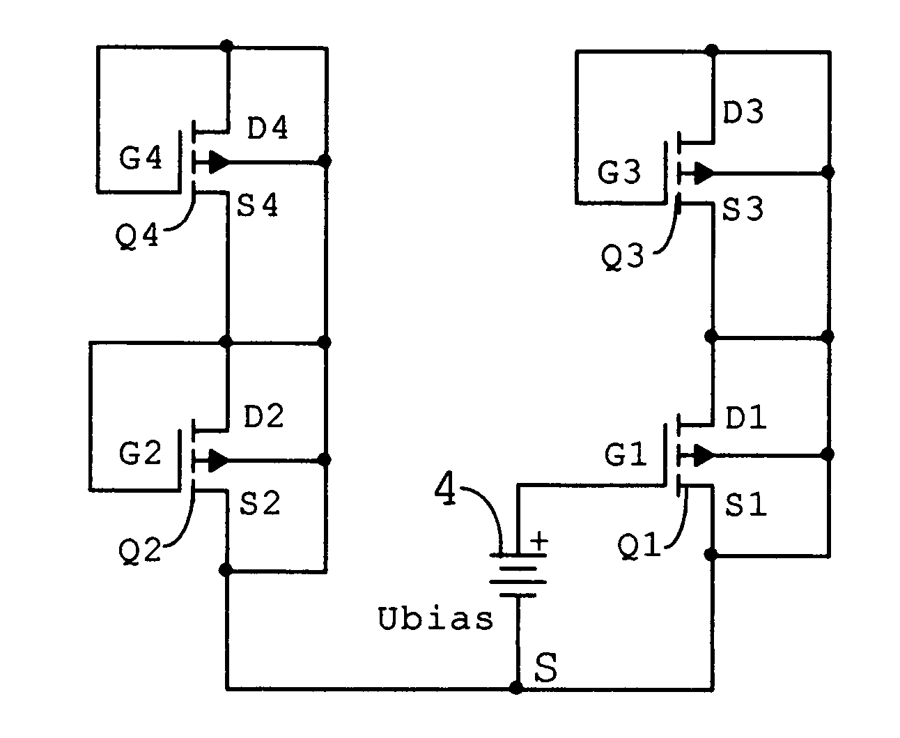
Personal dosimeter on the base of radiation integrated circuit.

a technology of integrated circuits and dosimeters, which is applied in the direction of radiation measurement, radiation intensity measurement, instruments, etc., can solve the problems of limited use of personal dosimeters, insufficient sensitive dosimeters for personnel workers in medical, nuclear and industrial fields, and a certain temperature coefficient of single radfets, etc., to achieve the effect of minimal temperature

US20110260070A1Inactive Publication Date: 2011-10-27URYUPIN FR OLEG +1
0 Cites 3 Cited by

Patent Information

Authority / Receiving Office
US · United States
Current Assignee / Owner
Publication Date
2011-10-27
Estimated Expiration
Not applicable · inactive patent

Smart Images

  • Figure 1
    Figure 1
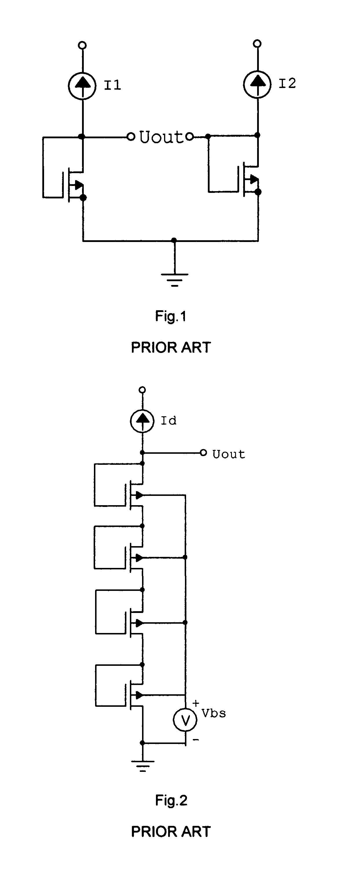
  • Figure 2
    Figure 2
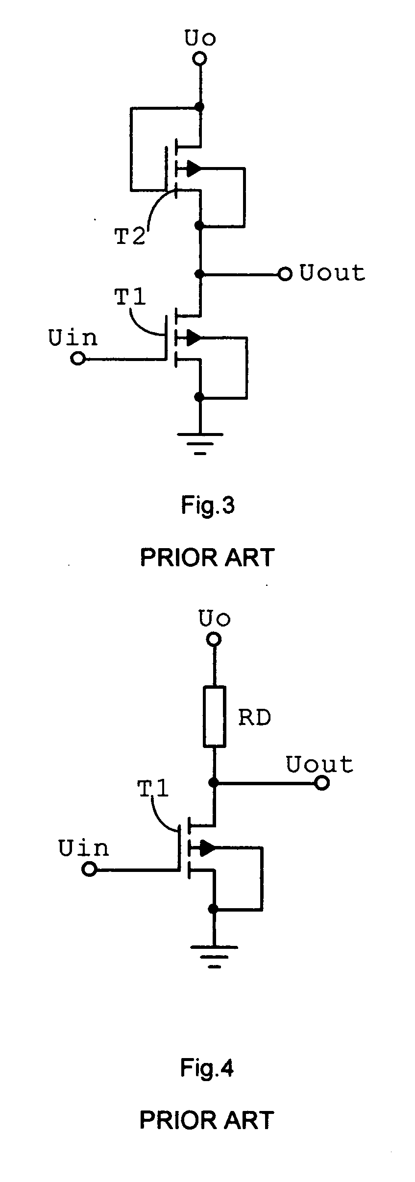
  • Figure 3
    Figure 3
Patent Text Reader

Abstract

This invention provides a radiation dosimeter and new method of operation which comprise two types of the metal-oxide-semiconductor field-effect transistor (MOSFET) circuits allowing to amplify the threshold voltage changes due to radiation and provide temperature compensation. The first type dosimeter is a radiation integrated circuit (RADIC) which includes two radiation field-effect transistors (RADFET) and two MOSFETs, integrated into the same substrate. The second type of radiation circuit includes two RADFETs, integrated into the same substrate, and two resistors. The amplification of the threshold voltage change is achieved by using amplification principles of an MOSFET inverter. In both cases, under the ionizing irradiation, the gate of first RADFET is forward biased and the gate of second RADFET is biased off. In the reading mode the amplified differential threshold voltage change is measured. The increased radiation sensitivity allows to measure of the milli-rad doses. The temperature effect and drift is substantially eliminated. These radiation integrated circuits can be used as a personal dosimeter in the nuclear, industrial and medical fields.
Need to check novelty before this filing date? Find Prior Art

Description

REFERENCES CITEDPatent Documents

[0001] Canadian Patent 1,204,885 5 / 1986 Ian ThomsonOTHER PUBLICATIONS

[0002] B. O'Connell, A. Kelleher, W. Lane, L. Adams, <<Stacked RADFETs for Increased Radiation Sensitivity>>, IEEE Tran. Nucl. Sci. Vol. 43, N3, June 1996, pp. 481-486.

[0003] V. Polischuk and G. Sarrabayrouse, <<MOS ionizing radiation dosimeters: from low to high dose measurement>>, Radiation Physics and Chemistry, Vol. 61, 2001, pp. 511-513.

[0004] G. Sarrabayrouse, D. Buchdahl V. Polischuk, S. Siskos, <<Stacked MOS ionizing radiation dosimeters: potentials and limitations>>, Radiation Physics and Chemistry, Vol. 71, 2003, pp. 737-739.

[0005] R. H. Crawford, “MOS FET in Circuit Design”, New York: McGraw-Hill. 1967.BACKGROUND OF THE INVENTION

[0006] Metal-oxide-semiconductor dosimeters are MOS field-effect transistors with a specially processed gate insulator in order to make it radiation soft.

[0007] There are presently conventional personnel dosimeters such...

Examples

Embodiment Construction

[0033]FIG. 3 shows an inverter made of two MOSFETs, where T1 is a managing MOSFET transistor and T2 is a loading MOSFET transistor. Amplification coefficient of this inverter according to a prior art from the book of R. H. Crawford referenced in background of the invention is

UoutUin=Au=-β1β2=-(W / doxL)1(W / doxL)2

Where β is given as

β=μɛoɛoxWdoxL

[0034]FIG. 4 shows an inverter made of a MOSFET and a resistor, where T1 is a managing transistor and RD is a loading resistor. Amplification coefficient of this second inverter according again to a prior art from the book of R. H. Crawford is proportional to steepness or transition conductivity and to the loading resistance:

UoutUin=Au=-gm(RDrd)

Where (RD∥rd) is an equivalent resistance of parallel connected loading resistor RD and dynamic drain resistance rd.

(RDrd)=RD⋆rdRD+rdgm=2β⋆ID

[0035]FIG. 5 illustrates the basic embodiment of the present invention. The RADFET Q2 has its gate G2, drain D2 and source S2 connected together and they are connect...