Semiconductor device and method of fabricating the same

Active Publication Date: 2011-10-27
INST OF MICROELECTRONICS CHINESE ACAD OF SCI
View PDF0 Cites 8 Cited by
  • Summary
  • Abstract
  • Description
  • Claims
  • Application Information

AI Technical Summary

Benefits of technology

[0005]In view of the above problems, it is an object of the present invention to provide a semiconductor device and a method of fabricating the same i

Problems solved by technology

However, conventional processes have many problems in fabricating the contacts whose size is increasingly reduced.
For example, in order to etch a small contact hole through a dielectric layer, a high bias is required for the reactive ion etching (RIE), which, however, results in a reduced etching sele

Method used


Image

  • Semiconductor device and method of fabricating the same
  • Semiconductor device and method of fabricating the same
  • Semiconductor device and method of fabricating the same

Examples


Embodiment Construction

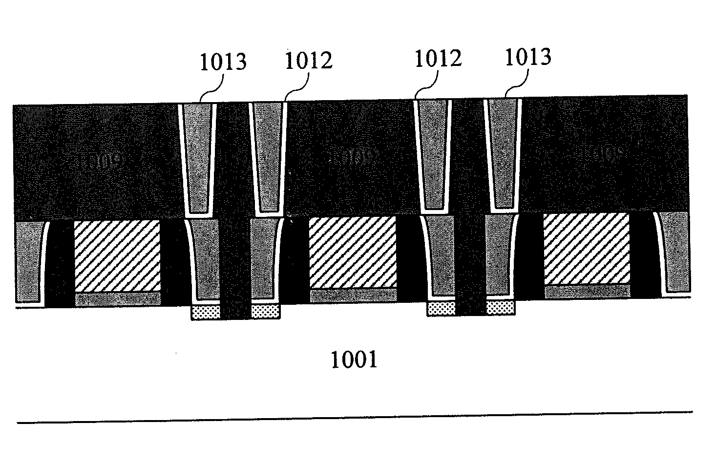
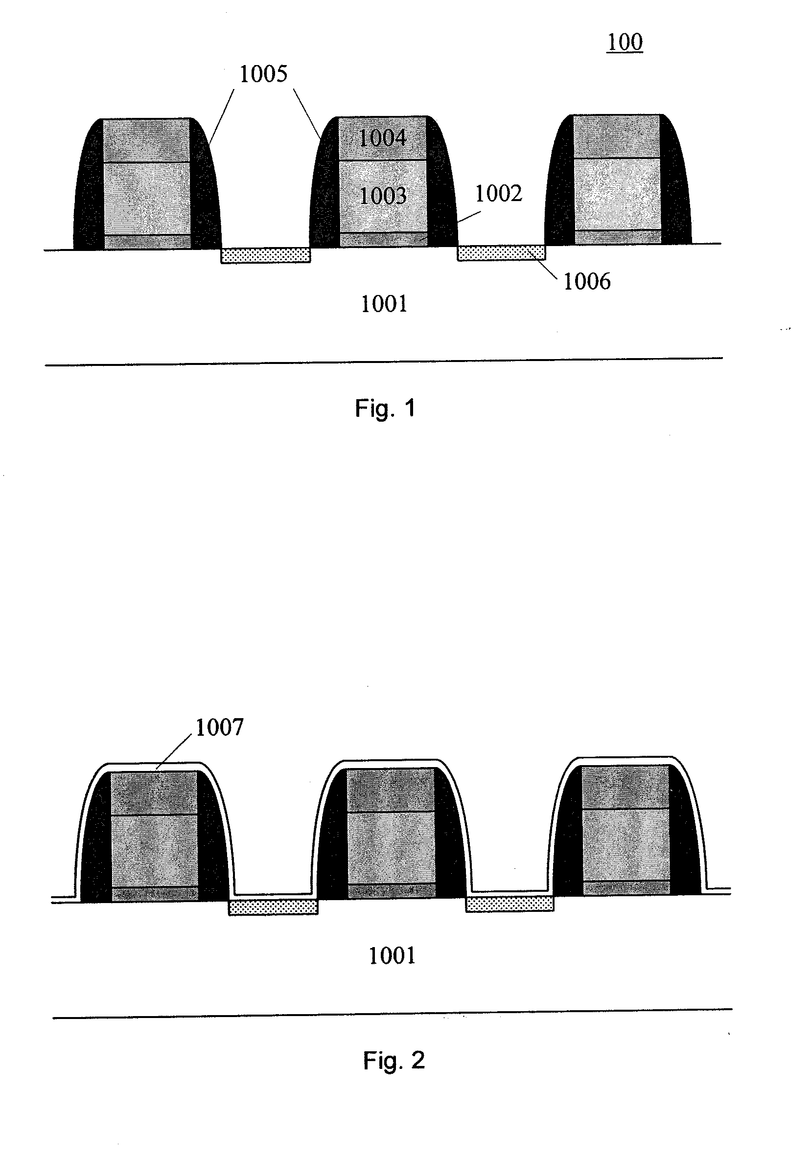
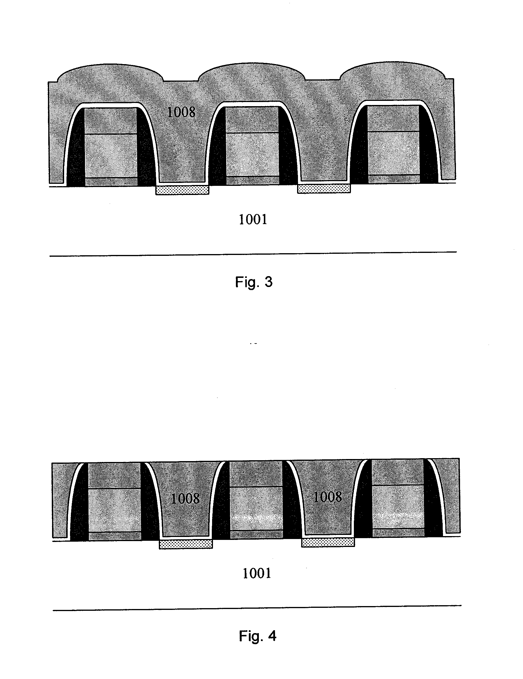
[0020]Hereinafter, the present invention is described with reference to embodiments shown in the attached drawings. However, it is to be understood that the descriptions are only provided for illustrative purpose, rather than limiting the present invention. Further, in the following, descriptions of known structures and techniques are omitted so as not to obscure the concept of the present invention.

[0021]In the drawings, various layer-structural diagrams according to embodiments of the present invention are shown. However, they are not drawn to scale, and some features may be enlarged while some features may be omitted for clarity. Shapes, sizes and relative positions of respective regions and layers shown in the drawings are only illustrative, and deviations therefrom may occur due to manufacture tolerances and technical limits. Those skilled in the art can also devise regions / layers of different shapes, sizes and relative positions as desired.

[0022]According to an embodiment of t...


PUM


Abstract

A semiconductor device includes a semiconductor substrate; gates, spacers on both sides of the respective gates, and source and gain regions on both sides of the respective spacers, which are formed on the semiconductor substrate; lower contacts located on the respective source and gain regions and abutting outer-sidewalls of the spacers, with bottoms covering at least a portion of the respective source and gain regions; an inter-layer dielectric layer formed on the gates, the spacers, the source and gain regions, and the lower contacts, wherein the respective source and gain regions of each of the transistor structures are isolated from each other by the inter-layer dielectric layer; and upper contacts formed in the inter-layer dielectric layer and corresponding to the lower contacts. Methods for fabricating such a semiconductor device and for manufacturing contacts for semiconductor devices.

Description

FIELD OF INVENTION[0001]The present invention generally relates to the field of integrated circuits fabrication, and more particularly, to a semiconductor device and a method of fabricating the same, and especially, to a contact of the semiconductor device and the fabrication of the contact.BACKGROUND[0002]With increasingly scaling of integrated circuits (IC's), contacts between respective layers of IC chips are becoming smaller and smaller. However, conventional processes have many problems in fabricating the contacts whose size is increasingly reduced. For example, in order to etch a small contact hole through a dielectric layer, a high bias is required for the reactive ion etching (RIE), which, however, results in a reduced etching selectivity in the RIE of the contact hole. In such a case, the RIE either causes an under-etching of the dielectric layer (with a low RIE bias), or an over-etching of the dielectric layer (with a high RIE bias).[0003]In order to solve the problem, ref...

Claims


Application Information

Patent Timeline
IPC IPC(8): H01L27/088H01L21/8232
CPCH01L21/76895H01L21/76897H01L21/823475H01L21/823468H01L21/823425H01L23/485H01L23/5226
Inventor YIN, HAIZHOULUO, ZHIJIONGZHU, HUILONG
Owner INST OF MICROELECTRONICS CHINESE ACAD OF SCI
Why Eureka
Try Eureka