Conductive structure and method of manufacturing the same

Active Publication Date: 2011-11-17
INNOCOM TECH SHENZHEN +1
View PDF3 Cites 58 Cited by
  • Summary
  • Abstract
  • Description
  • Claims
  • Application Information

AI Technical Summary

Benefits of technology

[0008]The disclosure is directed to a touch panel with the simpler

Problems solved by technology

In the processes of manufacturing the touch panel, however, the step of adhering the transparent cover layer via the optical adhesive makes the manufacturing processes become

Method used


Image

  • Conductive structure and method of manufacturing the same
  • Conductive structure and method of manufacturing the same
  • Conductive structure and method of manufacturing the same

Examples


first embodiment

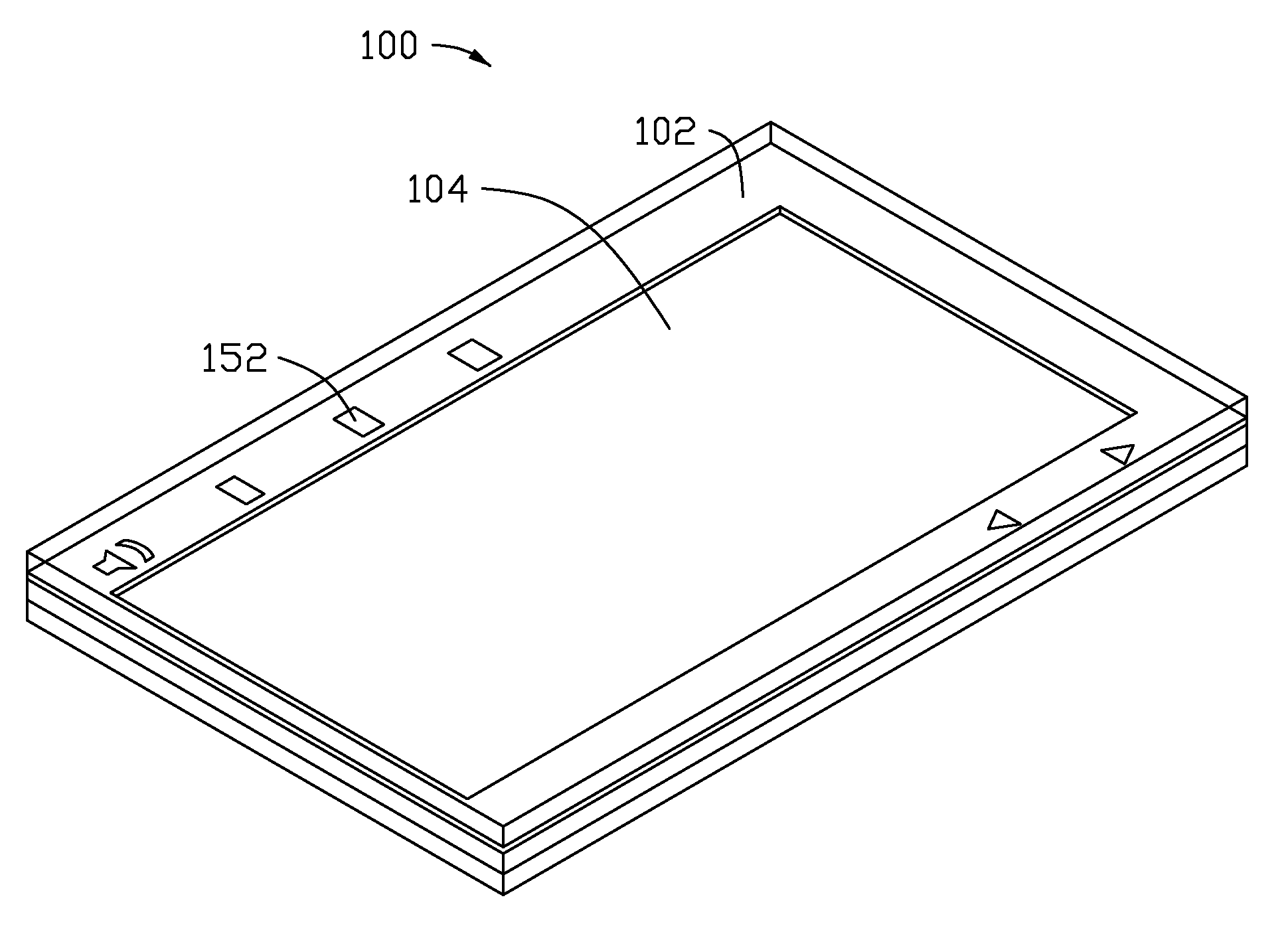
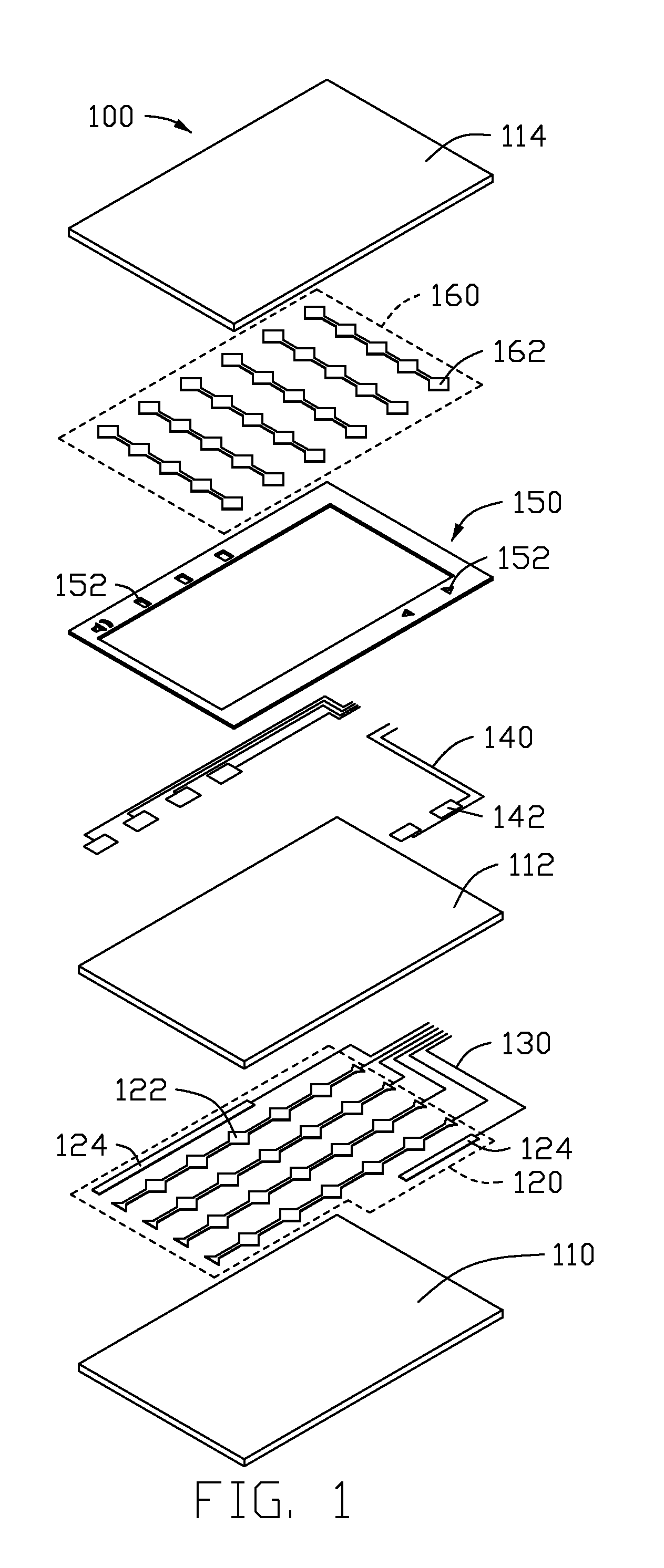
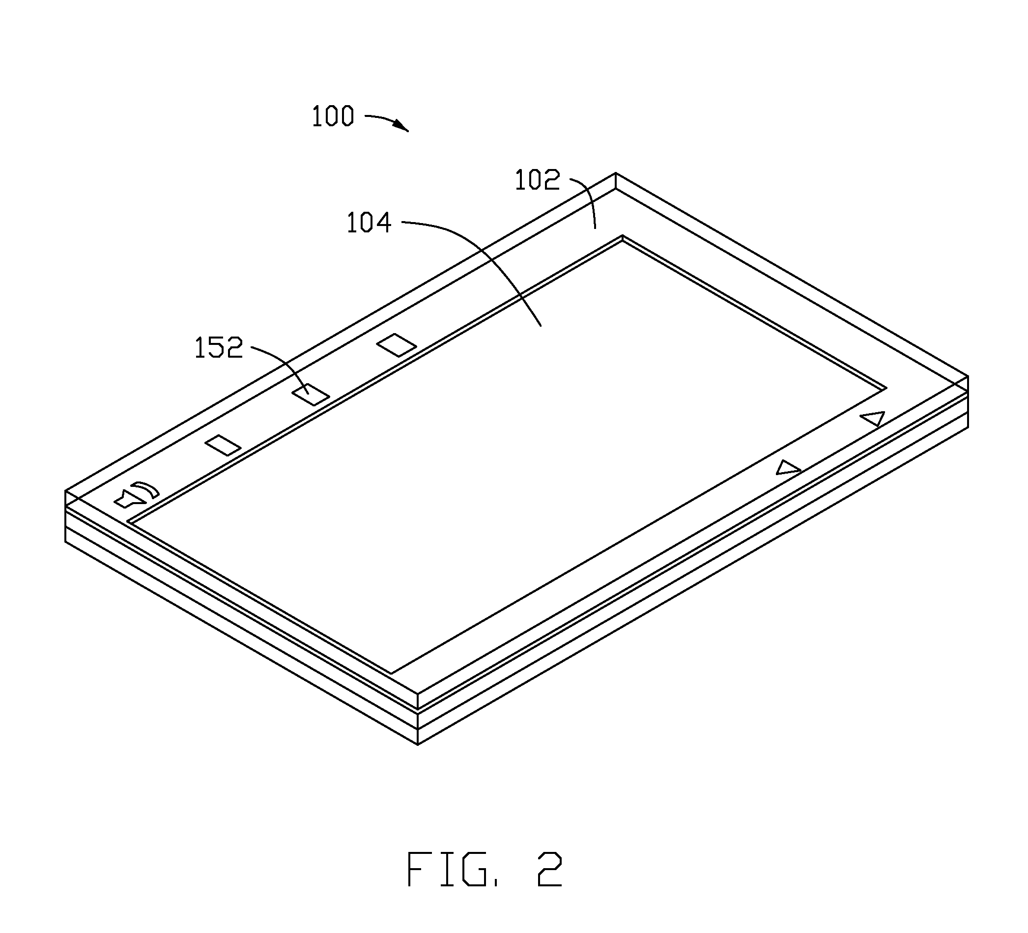
[0023]A touch panel according to the disclosure includes a substrate, a lower conductive layer disposed on the substrate, an insulating layer disposed on the lower conductive layer, a first conductive wire disposed on the insulating layer, a light shielding layer disposed on the first conductive wire, and an upper conductive layer disposed on the light shielding layer. The light shielding layer and the first conductive wire are located in an edge region of the touch panel in a planar view. The light shielding layer includes a first through hole. The upper conductive layer is electrically connected to the first conductive wire via the first through hole.

[0024]In the touch panel of the first embodiment, the upper conductive layer may be directly formed on a transparent cover layer so as to simplify the manufacturing processes and reduce the manufacturing cost.

second embodiment

[0025]A touch panel according to the disclosure includes a lower conductive layer, an insulating layer disposed on the lower conductive layer, an upper conductive layer disposed on the insulating layer and a transparent cover layer covering the upper conductive layer. A first conductive wire is further disposed on the insulating layer, and a light shielding layer is disposed on the first conductive wire. The light shielding layer includes a first through hole. The first conductive wire is electrically connected to the upper conductive layer via the first through hole. The light shielding layer and the first conductive wire are located in an edge region of the touch panel in a planar view. The upper and lower conductive layers overlap with each other in the edge region to form a first touch capacitor. The first through hole serves as a touch function control character of the first touch capacitor. When a position where the first through hole is located is touched, a capacitance of th...


PUM

PropertyMeasurementUnit
Timeaaaaaaaaaa
Volumeaaaaaaaaaa
Electrical conductoraaaaaaaaaa

Abstract

The disclosure relates to a touch panel, a method for manufacturing the same, and a touch display device using the same. The touch panel includes a substrate, a lower conductive layer disposed on the substrate, an insulating layer disposed on the lower conductive layer, at least one first conductive wire disposed on the insulating layer, a light shielding layer disposed on the first conductive wire, and an upper conductive layer disposed on the light shielding layer. The light shielding layer and the at least one first conductive wire are located in an edge region of the touch panel in a planar view. The light shielding layer includes at least one first through hole. The upper conductive layer is electrically connected to the at least one first conductive wire via the at least one first through hole.

Description

BACKGROUND OF THE DISCLOSURE[0001]1. Field of the Disclosure[0002]The disclosure relates in general to a touch panel, a method for manufacturing the touch panel, and a touch display device using the touch panel.[0003]2. Description of Related Art[0004]With the flourishing development of the flat panel display technology and the gradual decrease of the manufacturing cost, the flat panel display device advantageously having the low radiation, the thin thickness and the low power consumption gradually gets the favor of the consumer, and is thus widely applied to the electronic products. In order to satisfy the more convenient and directer requirement of the man-machine interface for the modern human beings, various flat panel display devices (i.e., touch display devices) having touch functions have been gradually available in the recent market. Usually, the touch display devices may be classified in to an external type and an internal type. The external type touch display device is to ...

Claims


Application Information

Patent Timeline
IPC IPC(8): G06F3/045H05K3/30
CPCG06F3/044Y10T29/4913G06F2203/04103G06F3/0445G06F3/0446
Inventor MENG, KAI
Owner INNOCOM TECH SHENZHEN
Why Eureka
Try Eureka