Organic light emitting display device and driving method thereof

Active Publication Date: 2011-11-17
SAMSUNG DISPLAY CO LTD
View PDF6 Cites 62 Cited by
  • Summary
  • Abstract
  • Description
  • Claims
  • Application Information

AI Technical Summary

Benefits of technology

[0038]According to an organic light emitting display device of an embodiment of the present invention and a method of driving the organic light emitting display device, it is possible to compensate for the threshold voltag

Problems solved by technology

The active matrix organic light emitting display device has the advantage of consuming low power, but has a problem that display is not uniform because the magnitude of current flowing through an organic light emitting element is changed due to a voltage difference between a gate and a drain of a driv

Method used


Image

  • Organic light emitting display device and driving method thereof
  • Organic light emitting display device and driving method thereof
  • Organic light emitting display device and driving method thereof

Examples


first embodiment

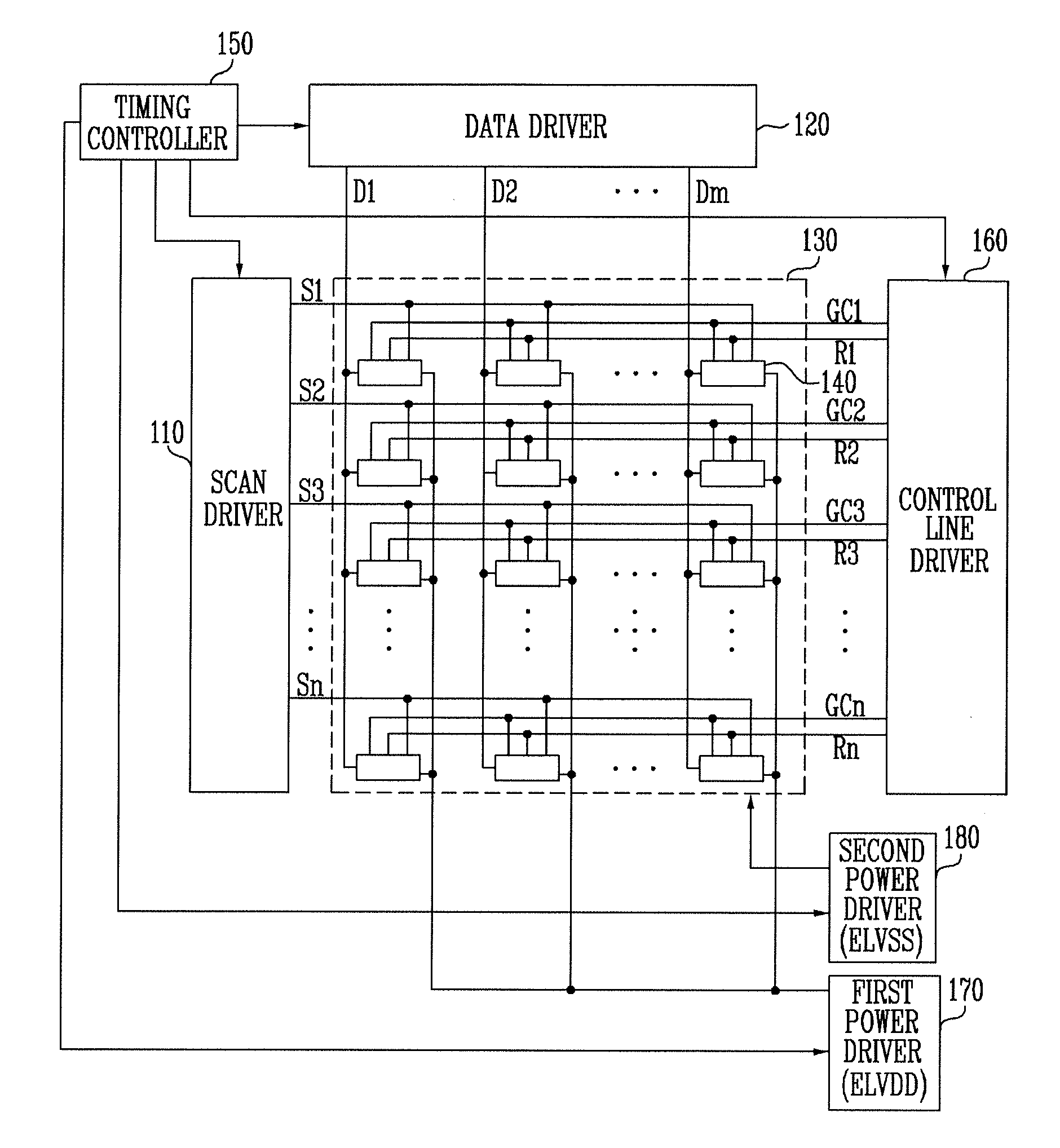
[0075]FIG. 5 is a circuit diagram illustrating a pixel shown in FIG. 1. The pixel coupled to the n-th scan line Sn and the m-th data line Dm is shown in FIG. 5, for the convenience of description. Further, it should be assumed that the organic capacitor Coled shown in FIG. 5 is a capacitor parasitically formed in the organic light emitting diode OLED. The organic capacitor Coled typically has a capacity larger than the first capacitor C1 (or the second capacitor C2).

[0076]Referring to FIG. 5, the pixel 140 according to the first embodiment of the present invention includes an organic light emitting diode OLED and a pixel circuit 142 for controlling the amount of current supplied to the organic light emitting diode OLED.

[0077]The anode electrode of the organic light emitting diode OLED is coupled to the pixel circuit 142 and the cathode electrode is coupled to the second power supply ELVSS. The organic light emitting diode OLED produces light with luminance (e.g., predetermined lumin...

second embodiment

[0095]FIG. 7 is a circuit diagram illustrating a configuration of the pixel shown in FIG. 1. In explaining FIG. 7, the same components as in FIG. 5 are designated by the same reference numerals and the detailed description thereof is not provided.

[0096]Referring to FIG. 7, a pixel 140′ according to the second embodiment of the present invention includes an organic light emitting diode OLED and a pixel circuit 142′ for controlling the amount of current supplied to the organic light emitting diode OLED. The pixel 140′, for example, may replace the pixel 140 of FIG. 1 according to embodiments of the present invention.

[0097]A first electrode of the fourth transistor M4′ included in the pixel circuit 142′ is coupled to a second electrode of the second transistor M2 and a second electrode is coupled to the first power supply ELVDD. Further, the gate electrode of the fourth transistor M4′ is coupled to a reset line Rn. The fourth transistor M4′ is turned on and electrically couples the fir...

third embodiment

[0100]FIG. 8 is a circuit diagram illustrating a configuration of the pixel shown in FIG. 1. In explaining FIG. 8, the same components as in FIG. 5 are designated by the same reference numerals and the detailed description thereof is not provided.

[0101]Referring to FIG. 8, a pixel 140″ according to the third embodiment of the present invention includes an organic light emitting diode OLED and a pixel circuit 142″ for controlling the amount of current supplied to the organic light emitting diode OLED. The pixel 140″, for example, may replace the pixel 140 of FIG. 1 according to embodiments of the present invention.

[0102]A first electrode of the fourth transistor M4″ included in the pixel circuit 142″ is coupled to a second electrode of the second transistor M2 and a second electrode and a gate electrode are coupled to the first power supply ELVDD. That is, the fourth transistor M4″ is diode-connected such that current can flow from the anode electrode of the organic light emitting di...


PUM


Abstract

An organic light emitting display device operating in a concurrent (e.g., simultaneous) emission method, which includes a first power driver configured to apply first power, which changes between a first low level and a first high level, to pixels of the display unit, and a second power driver configured to apply second power, which changes between a second low level and a second high level, to the pixels, wherein each of the pixels includes an organic light emitting diode, a driving transistor configured to control an amount of current supplied to the organic light emitting diode, and an initializing transistor coupled to an anode electrode of the organic light emitting diode and configured to be turned on during a reset period in one frame to supply a reset voltage, which is lower than the first high level of the first power, to the anode electrode of the organic light emitting diode.

Description

CROSS-REFERENCE TO RELATED APPLICATIONS[0001]This application claims priority to and the benefit of Korean Patent Application No. 10-2010-0044902, filed on May 13, 2010, in the Korean Intellectual Property Office, the entire content of which is incorporated herein by reference.BACKGROUND[0002]1. Field[0003]Embodiments of the present invention relate to an organic light emitting display device and a driving method thereof.[0004]2. Discussion of Related Art[0005]Recently, a variety of flat panel displays that makes it possible to reduce the faults, the weight, and the volume of cathode ray tubes, has been developed. Typical flat panel displays include liquid crystal displays, field emission displays, plasma display panels, and organic light emitting display devices, etc.[0006]The organic light emitting display device of the flat panel display devices displays an image using organic light emitting diodes that emit light by the recombination of electrons and holes, and has high response...

Claims


Application Information

Patent Timeline
IPC IPC(8): G09G5/10G09G3/30
CPCG09G3/003G09G3/3233G09G2300/043G09G3/3208G09G2300/0852G09G2300/0861G09G2300/0819
Inventor HAN, SANG-MYEONLEE, BAEK-WOON
Owner SAMSUNG DISPLAY CO LTD
Why Eureka
Try Eureka