Method for manufacturing dielectric isolation type semiconductor device

Inactive Publication Date: 2011-11-17
MITSUBISHI ELECTRIC CORP
View PDF0 Cites 2 Cited by
  • Summary
  • Abstract
  • Description
  • Claims
  • Application Information

AI Technical Summary

Benefits of technology

[0008]The present invention makes it possible to improve withst

Problems solved by technology

However, if a thick dielectric layer was locally formed on the major surface of a semic

Method used


Image

  • Method for manufacturing dielectric isolation type semiconductor device
  • Method for manufacturing dielectric isolation type semiconductor device
  • Method for manufacturing dielectric isolation type semiconductor device

Examples


Example

First Embodiment

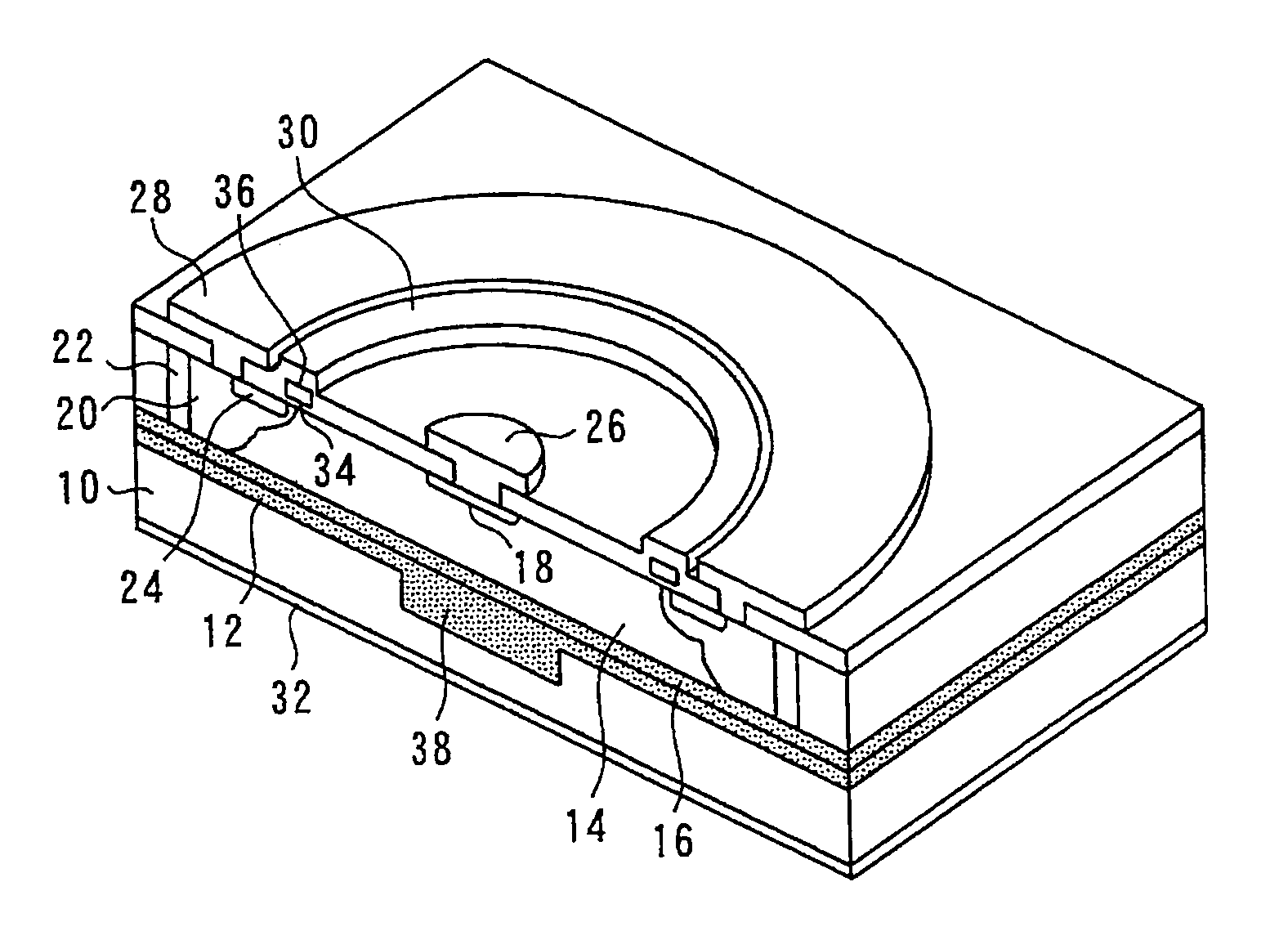
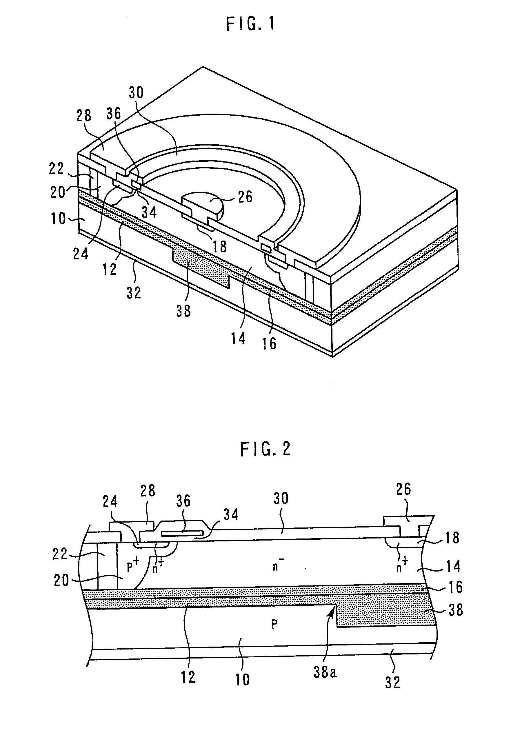
[0024]FIG. 1 is a sectional perspective view showing a dielectric isolation type semiconductor device according to the first embodiment; and FIG. 2 is a sectional view showing the main part of the dielectric isolation type semiconductor device according to the first embodiment.

[0025]A dielectric layer 12 is formed on the major surface of a p-type silicon substrate 10. A dielectric layer 16 is formed on the major surface of an n−-type semiconductor layer 14. The dielectric layer 12 and the dielectric layer 16 are tightly joined, and the n−-type semiconductor layer 14 is bonded to the major surface of a p-type silicon substrate 10. The dielectric layers 12 and 16 dielectrically separate the p-type silicon substrate 10 and the n−-type semiconductor layer 14.

[0026]An n+-type semiconductor region 18 having a higher impurity concentration than the n−-type semiconductor layer 14 is selectively formed on the surface of the n−-type semiconductor layer 14. A p+-type semiconduc...

Example

Second Embodiment

[0050]A method for manufacturing a dielectric isolation type semiconductor device according to the second embodiment will be described. The second embodiment differs from the first embodiment in the forming process of trenches 44 and the thick dielectric layer 38. FIGS. 12 to 14 are sectional view for illustrating the method for manufacturing the dielectric isolation type semiconductor device according to the second embodiment.

[0051]First, as shown in FIG. 12, a plurality of trenches 44 are formed on the region 42 in the major surface of the p-type silicon substrate 10. Here, the width α of the region between the trenches 44 is made to be smaller than 1 μm, and the opening part β of the trenches 44 is made to be about 1.5×α. Then, boron is rotation-implanted on the entire upper surface of the p-type silicon substrate 10 including the sidewalls and the bottoms of the trenches 44 and heat diffusion is conducted to form a p-type high-concentration diffusion region 46 i...

Example

Third Embodiment

[0056]A method for manufacturing a dielectric isolation type semiconductor device according to the third embodiment will be described. FIGS. 15 to 18 are sectional views for illustrating the method for manufacturing the dielectric isolation type semiconductor device according to the third embodiment.

[0057]First, in the same manner as in the first embodiment, a dielectric layer 12 and a thick dielectric layer 38 are formed on a p-type silicon substrate 10.

[0058]Next, as shown in FIG. 15, a plurality of trenches 52 are formed in the region 50 on the major surface of the n−-type semiconductor layer 14. Then, as shown in FIG. 16, the surface of the n−-type semiconductor layer 14 is oxidized by thermally oxidizing the entire wafer. Thereby, a dielectric layer 16 is formed on the major surface of the n−-type semiconductor layer 14, and a thick dielectric layer 54 is formed in the region 50. Thereafter, the surfaces of the dielectric layer 16 and the thick dielectric layer ...


PUM


Abstract

A method for manufacturing a dielectric isolation type semiconductor device comprises: forming a plurality of trenches in a first region on a major surface of a semiconductor substrate; forming a first dielectric layer on the major surface of the semiconductor substrate and a first thick dielectric layer in the first region by oxidizing a surface of the semiconductor substrate; bonding a semiconductor layer of a first conductive type to the semiconductor substrate via the first dielectric layer; forming a first semiconductor region by implanting an impurity into a part of the semiconductor layer above the first thick dielectric layer; forming a second semiconductor region by implanting an impurity of a second conductive type into a part of the semiconductor layer so as to surround the first semiconductor region separating from the first semiconductor region.

Description

BACKGROUND OF THE INVENTION[0001]1. Field of the Invention[0002]The present invention relates to a method for manufacturing a dielectric isolation type semiconductor device that can improve withstand voltage, and can prevent a semiconductor substrate from warping.[0003]2. Background Art[0004]In recent years, a dielectric isolation type semiconductor device wherein a semiconductor layer is bonded on a semiconductor substrate via a dielectric layer, and a power device is formed on the semiconductor layer has been proposed. However, in a conventional dielectric isolation type semiconductor device, the withstand voltage of the semiconductor device was limited depending on the thickness of the dielectric layer and the thickness of the semiconductor layer. In order to solve this problem, the formation of a thick dielectric layer locally on the major surface of a semiconductor substrate so as to contact the dielectric layer has been proposed (for example, refer to Japanese Patent Applicati...

Claims


Application Information

Patent Timeline
IPC IPC(8): H01L21/50
CPCH01L21/76251H01L21/76283H01L21/764H01L29/7824H01L21/02H01L27/12H01L29/786
Inventor AKIYAMA, HAJIME
Owner MITSUBISHI ELECTRIC CORP
Why Eureka
Try Eureka