Multilayered wiring structure, and method for manufacturing multilayered wiring

Inactive Publication Date: 2010-09-02
RENESAS ELECTRONICS CORP
View PDF2 Cites 17 Cited by
  • Summary
  • Abstract
  • Description
  • Claims
  • Application Information

AI Technical Summary

Benefits of technology

[0020]According to the present invention, the part of the surface of the interlayer insulation film in which an embedded wiring is formed is made higher at the central region of the interwiring and lower at the region adjacent to the wiring. Accordingly, the creepage distance between the wirings increases and thus the TDDB withstand voltage improves. At the same time, the top surface of the interlayer insulation f

Problems solved by technology

However, if there is a level difference, the focus margin during the exposure for forming a via hole on the upper insulation film is degraded, and thus, planarization by polishing the insulation film is esse

Method used


Image

  • Multilayered wiring structure, and method for manufacturing multilayered wiring
  • Multilayered wiring structure, and method for manufacturing multilayered wiring
  • Multilayered wiring structure, and method for manufacturing multilayered wiring

Examples


Example

Embodiment 1

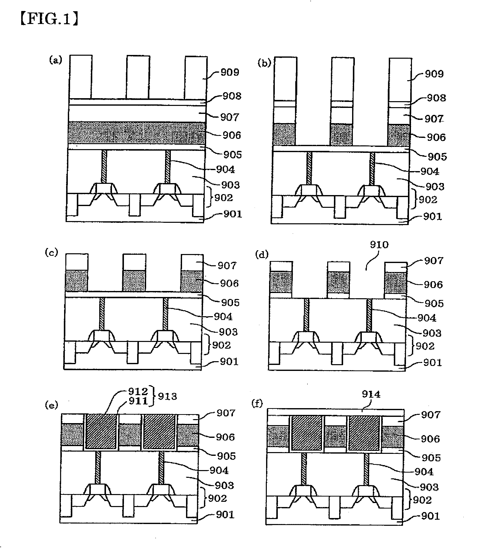
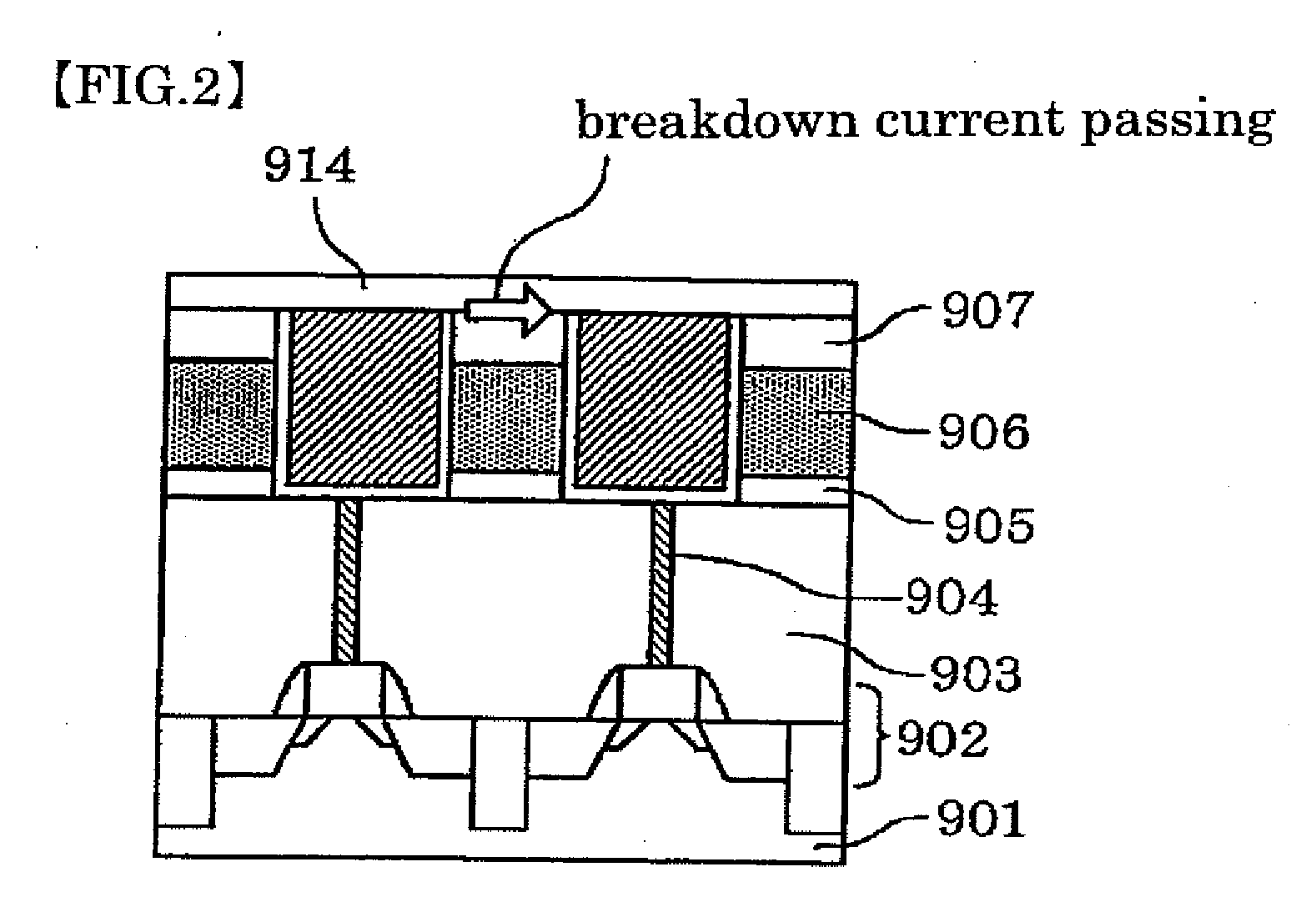
[0042]FIGS. 6A(a) to 6B(g) are sectional views that schematically illustrate each manufacturing process of the multilayered wiring structure according to Embodiment 1 of the present invention in the process sequence. In Embodiment 1, a Cu wiring is formed in the trench of the silicon oxide film / porous SiOCH film / silicon carbide-nitride film, and some part of the silicon oxide film is removed so that TDDB withstand voltage will improve. First, a MOS transistor 202, for example, is formed on the silicon substrate 201, and a silicon oxide film 203, for example, is formed as an interlayer insulation film to cover the transistor portion, so that a contact plug 204 that connects the transistor and the wiring portion is formed using tungsten, for example. Next, a silicon carbide-nitride film 205 is formed by means of, for example, the CVD method as an etching stopper of the interlayer insulation film. Further, a porous SiOCH film 206 is formed on the silicon carbide-nitride fil...

Example

Embodiment 2

[0047]FIGS. 7A(a) to 7B(g) are sectional views that schematically illustrate each manufacturing process of the multilayered wiring structure according to Embodiment 2 of the present invention in the process sequence. In FIGS. 5A and 5B, the parts equivalent to those in FIGS. 6A and 6B that represent Embodiment 1 are assigned the reference numerals the last two digits of which are shared in common, and thus, the redundant descriptions will be properly omitted. In Embodiment 2, a Cu wiring is formed in the trench of the silicon oxide film / porous SiOCH film / silicon carbide-nitride film, and further, an organic macromolecule film is formed on the side surface of the wiring trench. In addition, similar to Embodiment 1, a part of the silicon oxide film is removed whereby TDDB reliability improves.

[0048]First, the processes similar to FIGS. 6A(a) to 6A(c) showing Embodiment 1 are taken to form a trench in the silicon oxide film 307 and the porous SiOCH film 306 in which to embe...

Example

Embodiment 3

[0050]FIGS. 8A(a) to 8B(j) are sectional views that schematically illustrate each manufacturing process of the multilayered wiring structure according to Embodiment 3 of the present invention in the process sequence. In Embodiment 3, a so-called Dual Damascene Cu wiring is formed wherein the via hole and the wiring trench, both of which are formed in the insulation film structure composed of silicon oxide film / porous SiOCH / silicon oxide film / SiOCH / silicon carbide-nitride film, are simultaneously embedded. In addition, similar to Embodiment 1, a part of the silicon oxide film is removed whereby TDDB reliability improves.

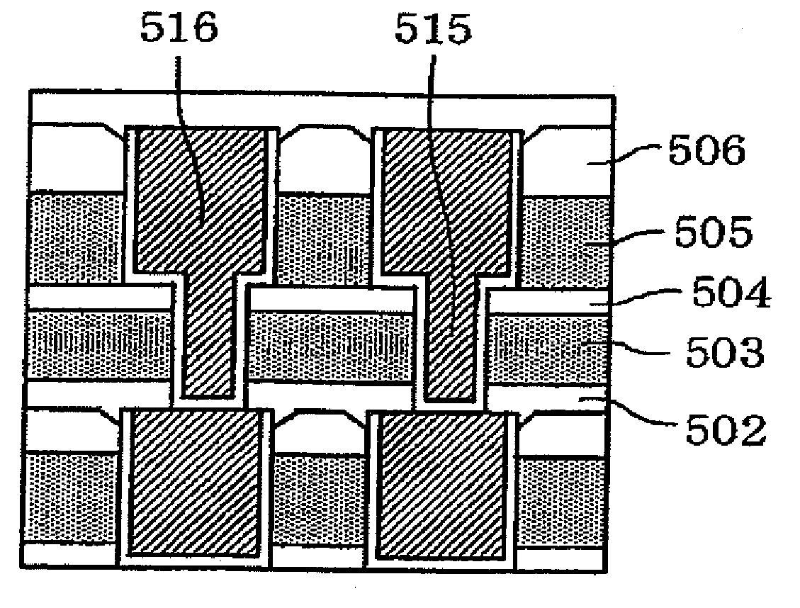
[0051]First, a SiOCH film 403, which will be a via hole interlayer insulation film, is formed on the top surface of the bottom wiring structure 401 by means of a silicon carbide-nitride film 402. The via hole interlayer film can be a porous SiOCH film, and further, a porous SiOCH film rigidized by UV irradiation or EB irradiation. Besides, a silicon oxide ...


PUM


Abstract

Provided is a wiring of the Damascene structure for preventing the TDDB withstand voltage degradation and for keeping the planarity to prevent the degradation of a focus margin. A trench wiring (213) is formed in an interlayer insulating film, which is composed of a silicon carbide-nitride film (205), a SiOCH film (206) and a silicon oxide film (207) [(e)]. The silicon oxide film (207) is etched at a portion adjacent to the wiring of a polished surface by dry etching or wet etching [(f)]. A silicon carbide-nitride film (SiCN) (214) is formed as a Cu cap film [(g)]. An interlayer insulating film is further formed thereon to form a conductive plug, a trench wiring and so on.

Description

BACKGROUND OF THE INVENTION[0001]1. Field of the Invention[0002]The present invention relates to a multilayered wiring structure and a method for manufacturing a multilayered wiring and, more particularly, to a method for manufacturing a multilayered wiring structure and a multilayered wiring having a trench wiring called Damascene structure.[0003]2. Description of the Related Art[0004]Aiming to more sufficiently describe the current technical level relating to the present invention, all of the patents, patent applications, patent publications, scientific articles and so on, which are cited or specified herein, are hereby incorporated by reference in their entirety.[0005]Recent VLSI devices require more than millions of elements to be integrated in a chip of several millimeters square, and thus, it is essential to miniaturize the elements and to manufacture miniaturized and a multilayered wiring. Here, particularly for faster operational velocity of the device, reduction in wiring r...

Claims


Application Information

Patent Timeline
IPC IPC(8): H01L23/522H01L21/768
CPCH01L21/76808H01L21/76814H01L21/7682H01L21/76834H01L21/76843H01L21/76849H01L2924/0002H01L23/53238H01L23/53295H01L2924/00
Inventor OOTAKE, HIROTOTAGAMI, MASAYOSHITADA, MUNEHIROHAYASHI, YOSHIHIRO
Owner RENESAS ELECTRONICS CORP
Why Eureka
Try Eureka