Nitride Compound Semiconductor and Process for Producing the Same

Inactive Publication Date: 2009-01-08
SUMITOMO CHEM CO LTD
View PDF12 Cites 1 Cited by
  • Summary
  • Abstract
  • Description
  • Claims
  • Application Information

AI Technical Summary

Benefits of technology

[0010]As a result of keen examinations to solve the above-described problems, the present inventors found that electrostatic withstand voltage was dramatic

Problems solved by technology

In the process of manufacturing a light emitting device wherein a light emitting element constituted as described above is incorporated, or in the situation of operating the light emitting device, if a large current flows instantaneously in the nitride compound semiconductor due to static electricity, a problem wherein the compound semiconductor is destroyed occurs.
However, in the above-described process for forming a non-doped layer at a temperature of 1050° C., the process for lamin

Method used


Image

  • Nitride Compound Semiconductor and Process for Producing the Same
  • Nitride Compound Semiconductor and Process for Producing the Same
  • Nitride Compound Semiconductor and Process for Producing the Same

Examples


Example

Example 1

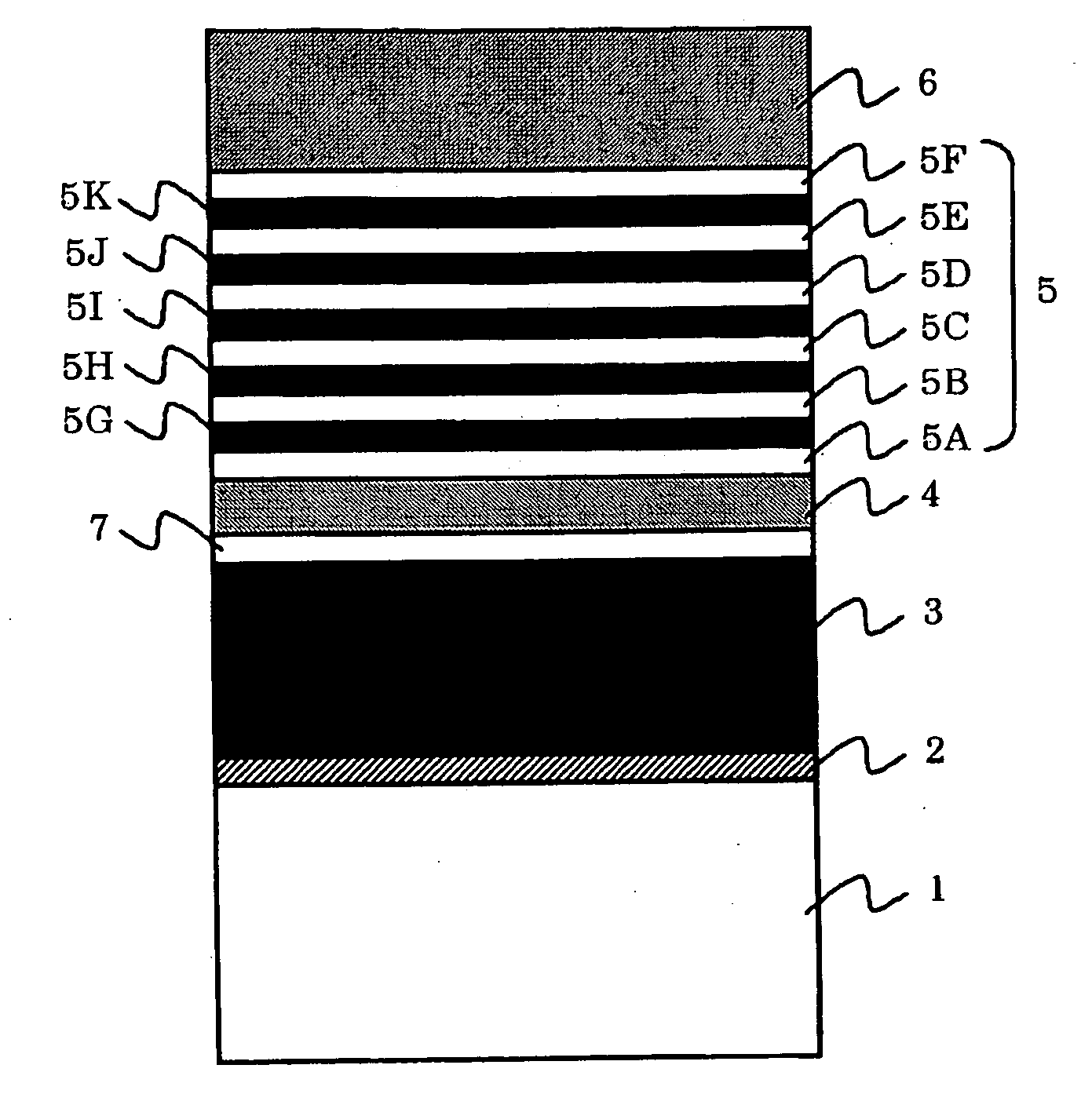
[0048]As a substrate, sapphire whose C surface was mirror polished was used. The process for growing a crystal was conducted by an MOVPE process, and a two-stage growth process using GaN grown at a low temperature was used as a buffer layer. The pressure in the growing furnace was set to 1 atmosphere, the substrate temperature was set at 550° C., hydrogen was used as the carrier gas, and TMG and ammonia was supplied to grow a GaN buffer layer of a thickness of about 50 nm.

[0049]Next, after elevating the substrate temperature to 1120° C., hydrogen carrier gas, TMG, silane and ammonia were supplied to grow an Si-doped n-type GaN layer of a thickness of about 4 μm, and supply of only silane was stopped to grow a non-doped GaN layer of a thickness of 300 nm.

[0050]Then, the substrate temperature was set at 780° C., the pressure in the growing furnace was set to 50 kPa, nitrogen was used as the carrier gas, and 610 sccm and 40 slm of TEG and ammonia, respectively, were supplied t...

Example

Example 2

[0057]An LED was fabricated in accordance with Example 1 except that the film thickness of the nitride semiconductor layer A was 200 nm. When a current of 20 mA was flowed in this LED in the forward direction, the LED exhibited clear blue light emitting. The electrostatic withstand voltage was 417 V.

Example

Example 3

[0058]An LED was fabricated in accordance with Example 1 except that the film thickness of the nitride semiconductor layer B was 150 nm. When a current of 20 mA was flowed in this LED in the forward direction, the LED exhibited clear blue light emitting. The electrostatic withstand voltage was 200 V.


PUM


Abstract

A process for producing a nitride compound semiconductor represented by a general formula, InxGayAlzN (where x+y+Z=1, 0≦x≦1, 0≦y≦1, and 0≦z≦1), characterized in that a non-doped nitride compound semiconductor (A) represented by a general formula, InaGabAlcN (where a+b+c=1, 0≦a≦1, 0≦b≦1, and 0≦c≦1) of a thickness of 500 to 5000 Å is formed between a p-type contact layer and an n-type contact layer at a temperature within a range between 550 and 850° C.

Description

TECHNICAL FIELD[0001]The present invention relates to a nitride compound semiconductor represented by a general formula, InxGayAlzN (where x+y+Z=1, 0≦x≦1, 0≦y≦1, and 0≦z≦1), and a process for producing the same.BACKGROUND ART[0002]In recent years, a light emitting element using a nitride compound semiconductor represented by a general formula, InxGayAlzN (where x+y+Z=1, 0≦x≦1, 0≦y≦1, and 0≦z≦1) has been incorporated and commercialized as a light source for a blue, green or white light emitting device. In this type of light emitting element, a nitride compound semiconductor layer is formed on a substrate such as a sapphire substrate.[0003]In the process of manufacturing a light emitting device wherein a light emitting element constituted as described above is incorporated, or in the situation of operating the light emitting device, if a large current flows instantaneously in the nitride compound semiconductor due to static electricity, a problem wherein the compound semiconductor is ...

Claims


Application Information

Patent Timeline
IPC IPC(8): H01L29/06H01L21/205H01L33/06H01L33/32H01L33/56H01L33/62
CPCH01L21/0237H01L21/0242H01L21/02458H01L21/0254H01L33/02H01L21/02579H01L21/0262H01L33/007H01L21/02576H01L2224/48091H01L2224/48247H01L2224/48257H01L2924/181H01L2924/00014H01L2924/00012
Inventor KASAHARA, KENJISASAKI, MAKOTOSHIMIZU, MASAYA
Owner SUMITOMO CHEM CO LTD
Why Eureka
Try Eureka