Electrophoretic display device, driving method therefor, and electronic apparatus

a display device and display device technology, applied in the direction of electric digital data processing, instruments, computing, etc., can solve the problems of short circuit between the first control electrode and the first electrode, and difficulty in full color display

Inactive Publication Date: 2011-11-24
SEIKO EPSON CORP
View PDF7 Cites 10 Cited by
  • Summary
  • Abstract
  • Description
  • Claims
  • Application Information

AI Technical Summary

Benefits of technology

[0054]According to this aspect, a display section that can perform smooth movement of particles and thus can perform color display in a stable manner is included. Therefore, at least any of the brightness, saturation, and hue of a displayed image can be controlled as appropriate.

Problems solved by technology

In the proposals disclosed in JP-A-2009-9092, JP-A-2007-98382, and JP-A-2003-186065, however, there are problems in terms of controllability of brightness and saturation in one subpixel for implementing a color electrophoretic display device, and therefore it is difficult to perform full color display.
If the first control electrode is formed in the same layer as the first electrodes, there is worry that a short-circuit between the first control electrode and the first electrodes would be made.

Method used


Image

  • Electrophoretic display device, driving method therefor, and electronic apparatus
  • Electrophoretic display device, driving method therefor, and electronic apparatus
  • Electrophoretic display device, driving method therefor, and electronic apparatus

Examples


first embodiment

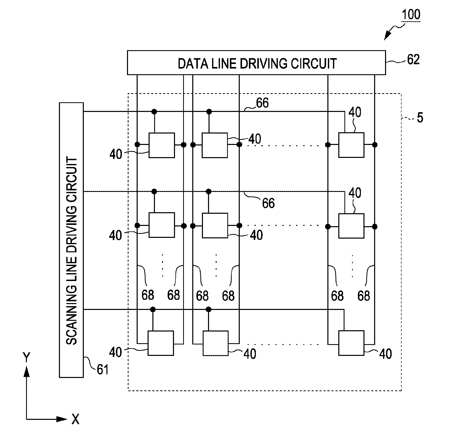
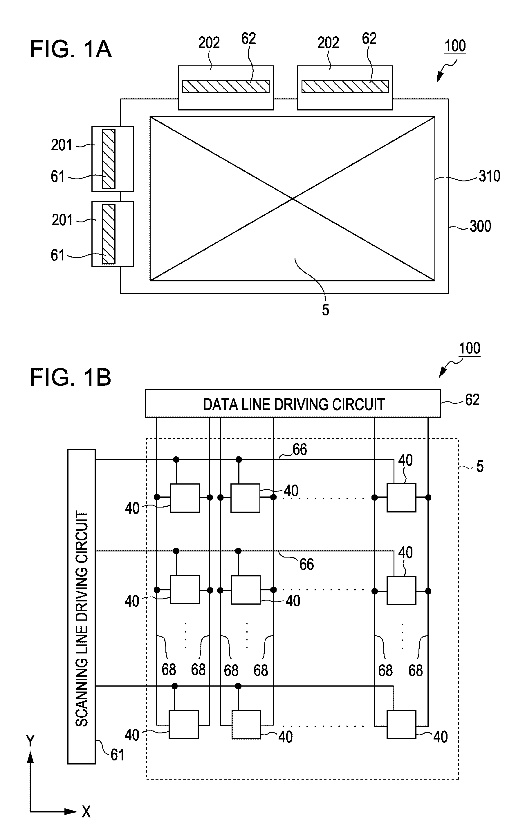
[0089]FIG. 1A is a plan view illustrating an overall configuration of an electrophoretic display device 100.

[0090]As illustrated in FIG. 1A, in the electrophoretic display device 100 of this embodiment, an element substrate 300 has a planar dimension larger than a counter substrate 310. On the element substrate 300 protruding more than the counter substrate 310, two scanning line driving circuits 61 and two data line driving circuits 62 are mounted as COF (Chip On Film) mountings (or TAB (Tape Automated Bonding) mounting) on flexible substrates 201 and 202 for connection with external devices. The flexible substrates 201 with the scanning line driving circuits 61 mounted thereon are mounted in a terminal-forming region that is formed on a peripheral edge along one short side of the element substrate 300, with an ACP (Anisotropic Conductive Paste), an ACF (Anisotropic Conductive Film), or the like therebetween. Here, the element substrate 300 is made of a first substrate 30 to be des...

second embodiment

[0218]Next, an electrophoretic display device of a second embodiment will be described.

[0219]FIG. 18 is a plan view illustrating a pixel structure of an electrophoretic display device of the second embodiment. FIG. 19 is a plan view illustrating a modification of the control electrode in the second embodiment.

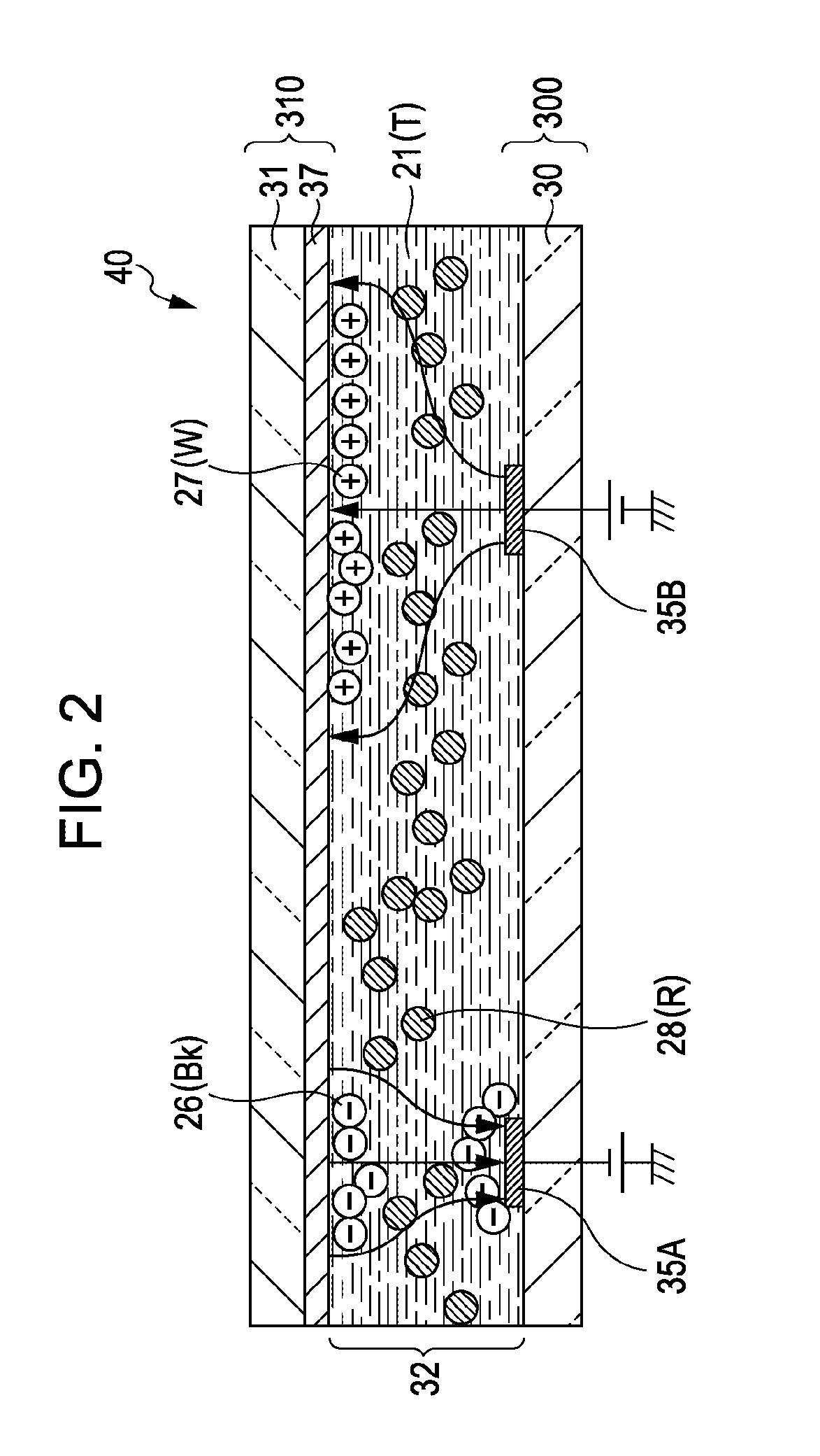
[0220]As illustrated in FIG. 18, the select transistors TR1 and TR2, the connecting electrodes 44A and 44B, the pixel electrodes 35A and 35B, and a control electrode 17 (a first control electrode) and a control electrode 18 (a second control electrode) are provided in each pixel 40 on the first substrate 30.

[0221]In the foregoing embodiment, one control electrode is provided in each pixel 40. However, in this embodiment, two control electrodes 17 and 18 are provided in each pixel 40. The control electrodes 17 and 18 are provided for the select transistors TR1, the connecting electrodes 44A, and the pixel electrodes 35A, the select transistor TR2, the connecting electrode 44B, a...

third embodiment

[0227]Next, an electrophoretic display device of a third embodiment will be described.

[0228]FIG. 20 is a partial sectional view illustrating a schematic structure of an electrophoretic display device of the third embodiment.

[0229]As illustrated in FIG. 20, the electrophoretic display device includes, on the first substrate 30, the select transistor TR1, which includes the gate electrode 41e, the gate insulating film 41b, the semiconductor layer 41a, the source electrode 41c, and the drain electrode 41d; and the connecting electrode 44B (44A), and the electrophoretic display device further includes the interlayer insulating film 42 formed above the first substrate 30 in such a manner as to cover these elements, the control electrode 18 (17) formed on the interlayer insulating film 42 and made of aluminum having a thickness of 300 nm, an interlayer insulating film 45 made of silicon nitride having a thickness of 300 nm and formed in such a manner as to cover the control electrode 18 (...


PUM

PropertyMeasurementUnit
thicknessaaaaaaaaaa
thicknessaaaaaaaaaa
thicknessaaaaaaaaaa

Abstract

An electrophoretic display device includes a first substrate and a second substrate, an electrophoretic layer disposed between the first substrate and the second substrate and containing at least a dispersion medium and positively or negatively charged particles mixed in the dispersion medium, first electrodes formed in island shapes and driven independently in respective pixels on a side of the electrophoretic layer of the first substrate, a second electrode formed on a side of the electrophoretic layer of the second substrate and having a larger area than the first electrodes, transistors connected to the first electrodes, and a first control electrode disposed in at least part of an area where the first electrodes are absent above a drain electrode of a first transistor of the transistors. A potential for repelling the particles is applied to the first control electrode.

Description

BACKGROUND[0001]1. Technical Field[0002]The present invention relates to electrophoretic display devices and driving methods therefor, and electronic apparatuses.[0003]2. Related Art[0004]In recent years, the use of electrophoretic display devices as display sections of electronic paper and the like has been spreading. An electrophoretic display device includes an electrophoretic dispersion liquid in which a plurality of electrophoretic particles are dispersed in a liquid phase dispersion medium (a dispersion medium). For the purpose of performing display, the electrophoretic display device utilizes the fact that application of an electric field causes the distribution state of electrophoretic particles to vary, and, as a result, the optical characteristics of the electrophoretic dispersion liquid vary.[0005]For such an electrophoretic display device, there has been proposed a concept of a color electrophoretic display device using three types of particles as disclosed in JP-A-2009-...

Claims


Application Information

Patent Timeline
Patent Type & Authority Applications(United States)
IPC IPC(8): G09G3/34G02F1/167G09G5/10G02F1/16762G02F1/16766
CPCG09G3/2003G09G3/3446G02F2001/1678G02F1/167G02F2001/1676G09G2300/0809G02F1/16762G02F1/16766
Inventor SATO, TAKASHI
Owner SEIKO EPSON CORP
Why Eureka
Try Eureka