Coil component and method of manufacturing the same

a technology of coil components and components, which is applied in the direction of magnets, inductances, magnetic bodies, etc., can solve the problems of high manufacturing cost, high manufacturing cost, and excessive filter performance specs, etc., and achieves the effect of easy manufacturing, low cost, and reduced manufacturing costs

Active Publication Date: 2011-12-01
TDK CORPARATION
View PDF5 Cites 71 Cited by
  • Summary
  • Abstract
  • Description
  • Claims
  • Application Information

AI Technical Summary

Benefits of technology

[0031]As described above, according to the present invention, a coil component that can be miniaturized, lowered, and manufactured at a low cost while securing desired filter performance can be provided. Also according to the present invention, a coil component ha...

Problems solved by technology

However, the structure of the conventional common mode filter uses upper and lower magnetic substrates made of ferrite and a ferrite substrate is easy to break when thinned too much, making slimming-down of the substrate difficult.
Further, the filter is made thicker by two magnetic substrates being stacked so that it has been difficult to provide a lowered chip component.
Moreover, a large amount of expensive magnetic materials is used, posing problems of high manufacturing costs and excessive specs of filter performance depending on uses.
In the conventional common mo...

Method used


Image

  • Coil component and method of manufacturing the same
  • Coil component and method of manufacturing the same
  • Coil component and method of manufacturing the same

Examples


first embodiment

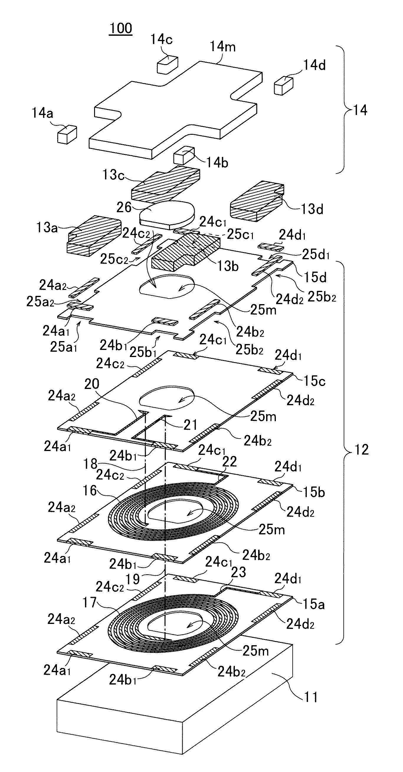
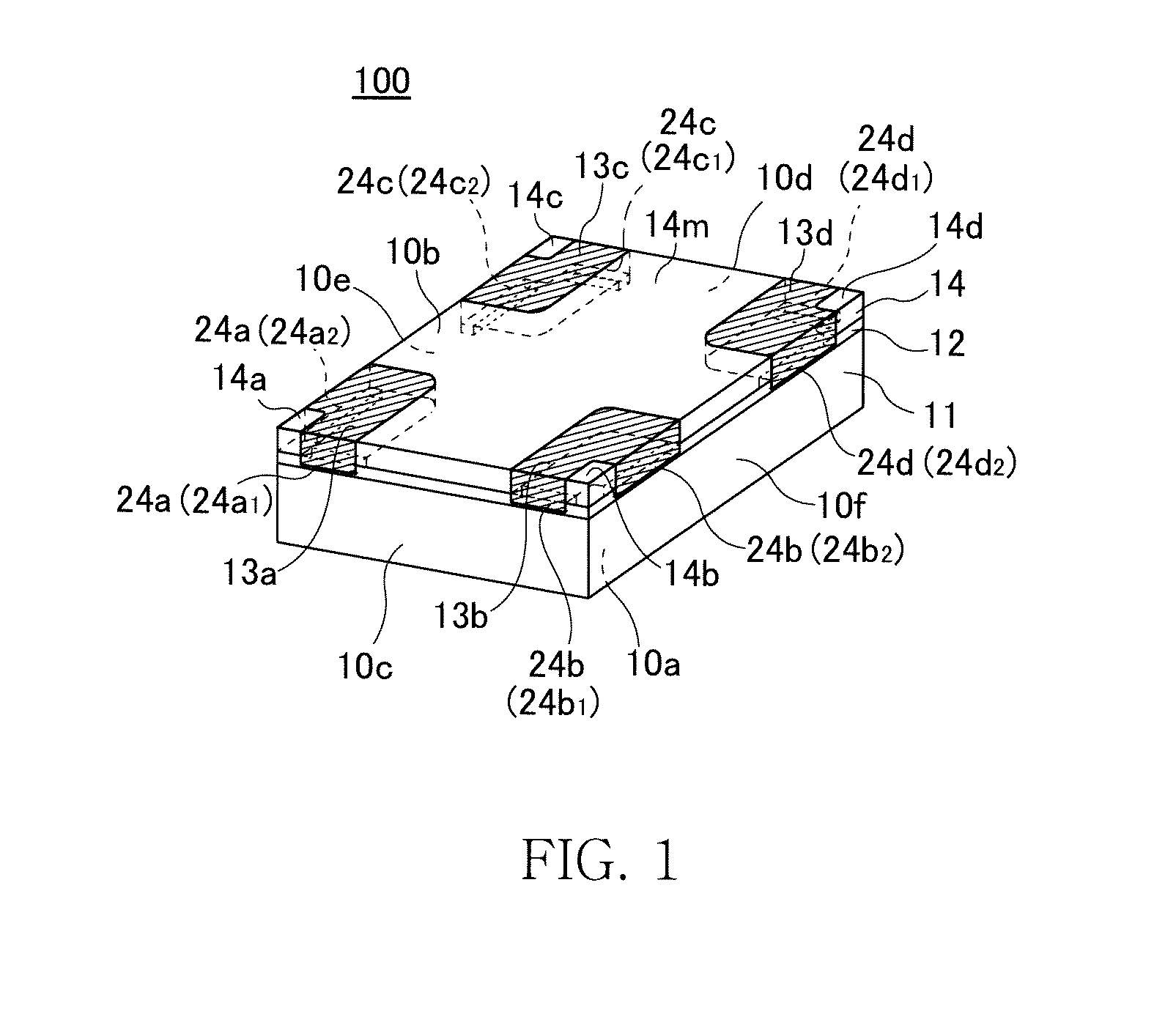
[0063]FIG. 1 is a schematic perspective view showing an appearance structure of a coil component 100 according to the present invention.

[0064]As shown in FIG. 1, the coil component 100 according to the present embodiment is a common mode filter and includes a magnetic substrate 11, a thin-film coil layer 12 containing a common mode filter element provided on one principal surface of the magnetic substrate 11, first to fourth bump electrodes 13a to 13d provided on the principal surface of the thin-film coil layer 12, and a magnetic resin layer 14 provided on the principal surface of the thin-film coil layer 12 excluding a formation position of the bump electrodes 13a to 13d. As illustrated in FIG. 1, the coil component 100 is a surface-mounted chip component in a shape of substantial rectangular parallelepiped and has an upper surface 10a, a bottom surface 10b, side surfaces 10c, 10d perpendicular to a longitudinal direction of the chip component, and side surfaces 10e, 10f in parall...

second embodiment

[0115]FIG. 12 is a schematic perspective view showing a structure of a coil component 200 according to the present invention.

[0116]As shown in FIG. 12, the coil component 200 according to the present embodiment is characterized in that the corner resin portions 14a to 14d are removed from the coil component 100 according to the first embodiment. Thus, in the corner of each of the bump electrodes 13a to 13d, a notch portion 13r of the bump electrode appears. The other configuration is substantially the same as the configuration of the coil component 100 and thus, the same reference numerals are attached to the same structural elements and the detailed description is omitted. Like the coil component 100 according to the first embodiment, the coil component 200 according to the present embodiment can increase fixing strength during soldering while preventing a short-circuit between bump electrodes by a solder bridge. Particularly even a portion covered with the corner resin portion is ...

third embodiment

[0118]FIG. 13 is a schematic perspective view showing the structure of a coil component 300 according to the present invention.

[0119]As shown in FIG. 13a, the coil component 300 according to the present embodiment is different from the coil component 200 according to the second embodiment in that the corner resin portions 14a to 14d are not present and further, no notch portion as a formation region of the corner resin portions 14a to 14d shown in the coil component 200 of the second embodiment is present. That is, each of the bump electrodes 13a to 13d is formed in the entire corner including the tip. With such a shape of the bump electrode, the terminal electrodes 24a, 24b have one L-shaped electrode shape having the exposure surface on two side surfaces.

[0120]As shown in FIG. 13a, if the bump electrode is formed in the entire corner, a burr of the bump electrode is more likely to arise during individualization of chip components. However, an occurrence burrs of the bump electrode...


PUM

PropertyMeasurementUnit
Lengthaaaaaaaaaa
Shapeaaaaaaaaaa
Widthaaaaaaaaaa

Abstract

A coil component is provided with a magnetic substrate made of magnetic ceramic material, a thin-film coil layer containing a coil conductor formed on one principal surface of the magnetic substrate, a plurality of bump electrodes formed on the principal surface of the thin-film coil layer, and an insulating resin layer formed on the principal surface of the thin-film coil layer excluding formation positions of the bump electrodes. Each bump electrode has an exposure surface on a bottom surface and on two side surfaces of a layered product composed of the magnetic substrate, the thin-film coil layer and the insulating resin layer. A corner of the each bump electrode has a notch portion. The insulating resin layer includes a center resin portion provided in a center of the principal surface of the thin-film coil layer and a plurality of corner resin portions provided in the notch portion of each bump electrode.

Description

TECHNICAL FIELD[0001]The present invention relates to a coil component and a method of manufacturing the coil component, and more particularly relates to a structure of a thin-film common mode filter containing a coil conductor and a manufacturing method thereof.BACKGROUND OF THE INVENTION[0002]In recent years, standards of USB 2.0 and IEEE1394 are widely distributed as high-speed signal transmission interfaces and used in a large number of digital devices such as personal computers and digital cameras. These interfaces adopt the differential transmission method that transmits a differential signal by using a pair of signal lines to realize faster signal transmission than the conventional single end transmission method.[0003]A common mode filter is widely used as a filter to remove noise on a high-speed differential transmission line. The common mode filter has characteristics that the impedance to a differential component of signals transmitted through a pair of signal lines is low...

Claims


Application Information

Patent Timeline
IPC IPC(8): H01F5/04H01F7/06
CPCH01F17/0013H01F5/003H01F27/292H01F17/04Y10T29/4902
Inventor OKUMURA, TAKESHIITO, TOMOKAZU
Owner TDK CORPARATION
Why Eureka
Try Eureka