Liquid crystal display device and method for driving liquid crystal display device

a liquid crystal display and display device technology, applied in static indicating devices, instruments, non-linear optics, etc., can solve the problems of inability to reduce power consumption and waste of backlight energy, and achieve the effect of suppressing display degradation caused by liquid crystal display devices such as color break, reducing eye strain such as flicker, and increasing the frequency of image signal input to each pixel of liquid crystal display devices

Active Publication Date: 2012-01-05
SEMICON ENERGY LAB CO LTD
View PDF6 Cites 29 Cited by
  • Summary
  • Abstract
  • Description
  • Claims
  • Application Information

AI Technical Summary

Benefits of technology

[0021]According to the one embodiment, the liquid crystal display device can be driven at high speed so that light emitted from the light source used for the backlight is not recognized by human eyes. Thus, a cause of eye strain such as a flicker can be reduced.
[0022]According to the liquid crystal display device which is one embodiment of the present invention, input of an image signal and lighting of a backlight are not performed sequentially in the whole pixel portion, but can be performed sequentially in every given region of the pixel portion, simultaneously in every region. Thus, the fr...

Problems solved by technology

In a liquid crystal display device expressing color tones by control of transmission of light emitted from a backlight source with u...

Method used


Image

  • Liquid crystal display device and method for driving liquid crystal display device
  • Liquid crystal display device and method for driving liquid crystal display device
  • Liquid crystal display device and method for driving liquid crystal display device

Examples


embodiment 1

[0048]In this embodiment, a liquid crystal display device which is one embodiment of the present invention will be described with reference to FIGS. 1A and 1B, FIGS. 2A to 2C, FIGS. 3A to 3D, FIGS. 4A and 4B, FIGS. 5A and 5B, and FIG. 6.

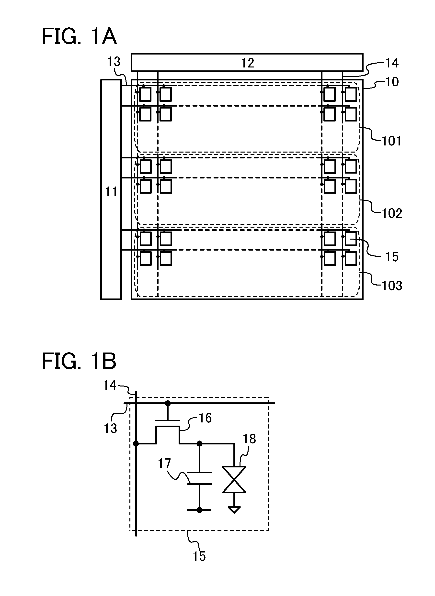
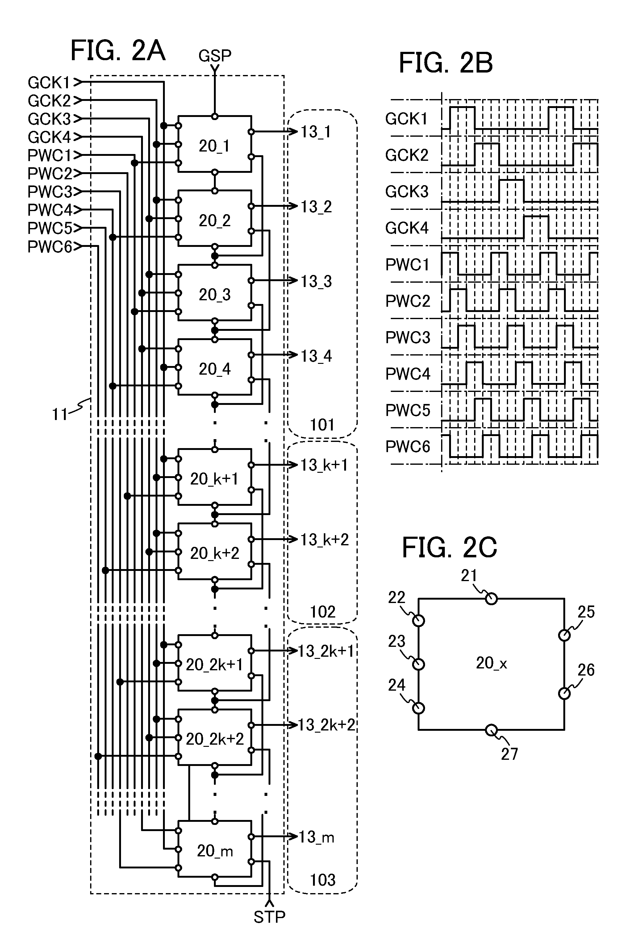
[0049]FIG. 1A illustrates a structural example of a liquid crystal display device. The liquid crystal display device illustrated in FIG. 1A includes a pixel portion 10, a scan line driver circuit 11, a signal line driver circuit 12, m scan lines 13 arranged in parallel or in substantially parallel to each other, whose potentials are controlled by the scan line driver circuit 11, and n signal lines 14 arranged in parallel or substantially in parallel to each other, and whose potentials are controlled by the signal line driver circuit 12. The pixel portion 10 is divided into three regions (regions 101 to 103), and each region includes a plurality of pixels arranged in a matrix. Each scan lines 13 is electrically connected to n pixels in each row, among...

embodiment 2

[0144]In this embodiment, a specific structure of the liquid crystal display device described in Embodiment 1 will be described.

[0145]First, specific examples of transistors used in a pixel portion or circuits used in the above liquid crystal display device are described with reference to FIGS. 17A to 17D. Note that in the liquid crystal display device, transistors provided in the pixel portion and the circuits may have the same structure or structures different from each other.

[0146]A transistor 2450 illustrated in FIG. 17A includes a gate layer 2401 over a substrate 2400, a gate insulating layer 2402 over the gate layer 2401, a semiconductor layer 2403 over the gate insulating layer 2402, and a source layer 2405a and a drain layer 2405b over the oxide semiconductor layer 2403. An insulating layer 2407 is formed over the semiconductor layer 2403, the source layer 2405a, and the drain layer 2405b. A protective insulating layer 2409 may be formed over the insulating layer 2407. The t...

embodiment 3

[0215]In this embodiment, one mode of a substrate used in the liquid crystal display device according to one embodiment of the present invention will be described with reference to FIGS. 23A to 23E and 23C′ to 23E′ and FIGS. 24A to 24C.

[0216]First, over a manufacturing substrate 6200, a layer 6116 to be separated from the manufacturing substrate 6200 and including components necessary for an element substrate, such as a transistor, an interlayer insulating film, a wiring, and a pixel electrode, is formed with a separation layer 6201 separating the layer 6116 from the manufacturing substrate 6200.

[0217]The manufacturing substrate 6200 may be a quartz substrate, a sapphire substrate, a ceramic substrate, a glass substrate, a metal substrate, or the like. Note that the substrate has a thickness sufficient for not exhibiting excessive flexibility, whereby an element such as a transistor can be formed with high accuracy. The description “the substrate has a thickness sufficient for not e...


PUM


Abstract

An object of the invention is to suppress degradation in image quality of a liquid crystal display device which performs display by field sequential method and to reduce power consumption of a backlight. The highest brightness of a first color light in a pixel region is detected. Gamma correction is performed so that transmittance of a pixel of the region displaying the highest brightness of the first color light is set to maximum and transmittance of other pixel of the region is decreased in accordance with lowering of the first color light intensity, and the region is irradiated with the highest brightness of the first color light. Similarly, a second color light is irradiated in another region concurrently with irradiation of the first color, whereby input of an image signal and lighting of the backlight are performed simultaneously in every region of the pixel portion.

Description

TECHNICAL FIELD[0001]The present invention relates to a method for driving a liquid crystal display device. In particular, the present invention relates to a field-sequential driving method of a liquid crystal display device.BACKGROUND ART[0002]A color filter method and a field sequential method are known as display methods for liquid crystal display devices. In a liquid crystal display device in which images are displayed by a color filter method, a plurality of subpixels each having a color filter that only transmits light with a wavelength of a given color (e.g., red (R), green (G), or blue (B)) are provided in each pixel. A desired color is produced in such a manner that transmission of white light is controlled in each subpixel and a plurality of colors are mixed in each pixel. On the other hand, in a liquid crystal display device in which images are displayed by a field sequential method, a plurality of light sources that emit lights of different colors (e.g., red (R), green (...

Claims


Application Information

Patent Timeline
IPC IPC(8): G02F1/1335
CPCG09G3/342G09G2310/0235G09G3/3677G09G3/3648
Inventor YAMAZAKI, SHUNPEIHIRAKATA, YOSHIHARUKOYAMA, JUN
Owner SEMICON ENERGY LAB CO LTD
Why Eureka
Try Eureka