Test mode control circuit in semiconductor memory device and test mode entering method thereof

a control circuit and memory device technology, applied in the direction of information storage, static storage, digital storage, etc., can solve the problem of unintentional operation mode satisfaction of the entering condition of the test mode during a user mode, and achieve the effect of minimizing or eliminating the failure of parallel bit operation entry

Active Publication Date: 2012-01-05
SAMSUNG ELECTRONICS CO LTD
View PDF5 Cites 10 Cited by
  • Summary
  • Abstract
  • Description
  • Claims
  • Application Information

AI Technical Summary

Benefits of technology

[0008]One or more embodiments may provide a semiconductor memory device that is capable of eliminating or minimizing parallel bit operation entry failure due to a boot failure when a built-in parallel bit (PBT) test is executed.
[0011]One or more embodiments provide a test mode control circuit and a test mode entry method in a semiconductor memory device that is capable of eliminating or minimizing parallel bit operation entry failure due to a boot failure when a built-in PBT is executed in a data processing system having a cache function.
[0012]One or more embodiments provide a test mode control circuit and a test mode entry method in a dynamic random access memory (DRAM) that is capable of preventing invalid TRMS entry during a normal operation and overcoming PBT operation entry failure due to a boot failure during a built-in PBT operation.

Problems solved by technology

Although an entering condition of the test mode can be accidentally satisfied by a signal noise or mistake while in a user mode, satisfaction of the entering condition of the test mode during a user mode is an unintentional operation mode.

Method used


Image

  • Test mode control circuit in semiconductor memory device and test mode entering method thereof
  • Test mode control circuit in semiconductor memory device and test mode entering method thereof
  • Test mode control circuit in semiconductor memory device and test mode entering method thereof

Examples


Embodiment Construction

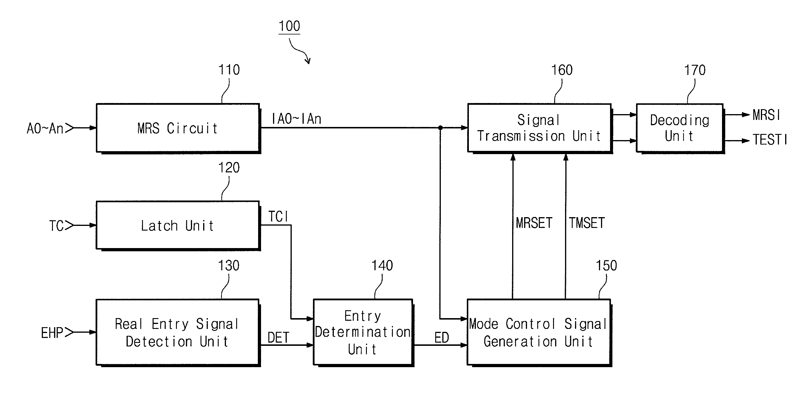
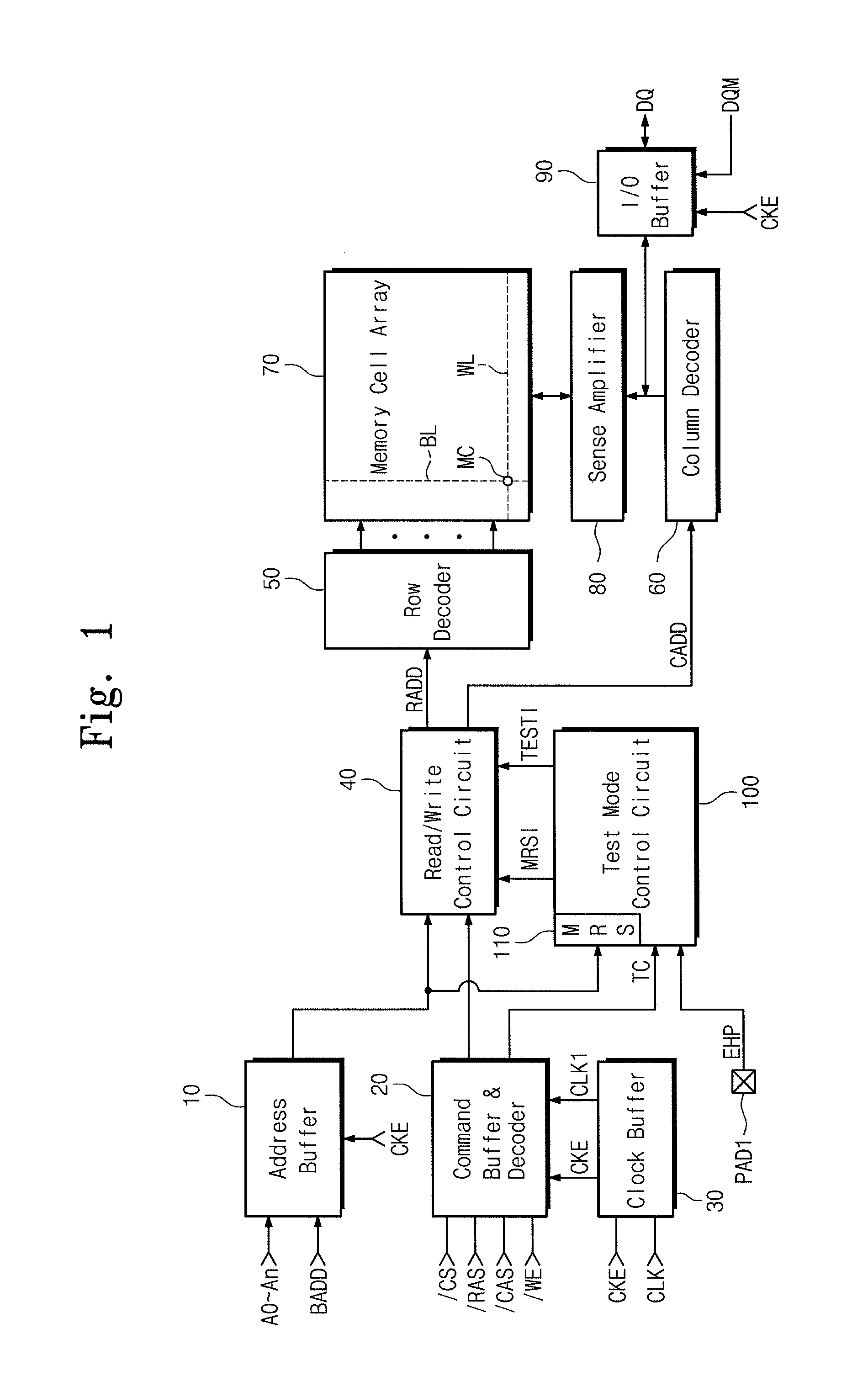
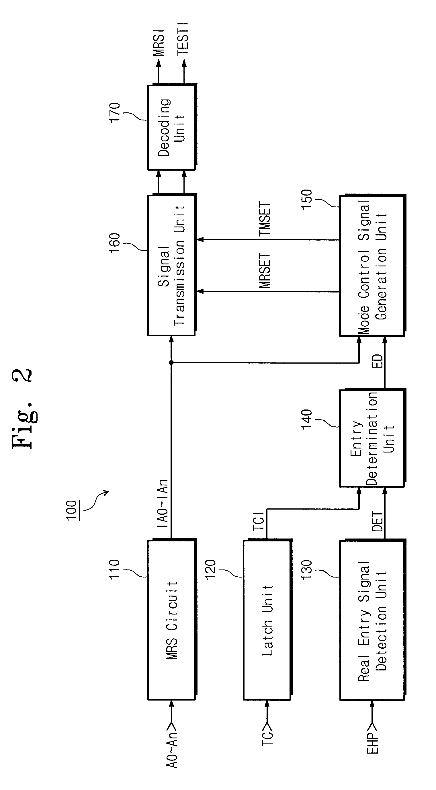
[0047]Exemplary embodiments will now be described more fully hereinafter with reference to the accompanying drawings; however, they may be embodied in different forms and should not be construed as limited to the embodiments set forth herein. Rather, these embodiments are provided so that this disclosure will be thorough and complete, and will fully convey the scope of the invention to those skilled in the art.

[0048]In the drawing figures, the dimensions of layers and regions may be exaggerated for clarity of illustration. It will be understood that when a layer or element is referred to as being “connected to” or “coupled to” another element, the elements may be directly connected or coupled to each other element or one or more intervening elements may be present. It is to be noted that the same or similar reference numerals are applied to the same or similar parts and elements throughout the specification and drawings. In some drawings, connection relationships between an element ...


PUM


Abstract

A test mode control circuit is provided to strictly allow entry into a test mode or prevent a boot failure from occurring during a boot operation for a built-in parallel bit test. The test mode control circuit includes a latch, a real entry signal detector, an entry determinator, and a mode control signal generator. When a real entry signal is detected, the entry signal determinator generates an entry determination signal and a test mode control signal is obtained from the mode control signal generator.

Description

CROSS-REFERENCE TO RELATED APPLICATIONS[0001]This application claims priority under 35 U.S.C. §119 to Korean Patent Application No. 10-2010-0064407, filed on Jul. 5, 2010, in the Korean Intellectual Property Office, and entitled: “Test Mode Control Circuit In Semiconductor Memory Device and Test Mode Entering Method Thereof,” which is incorporated by reference herein in its entirety.BACKGROUND[0002]1. Field[0003]Embodiments relate to semiconductor memory devices and, more particularly, to a test mode control circuit in a semiconductor memory device and a test mode entering method thereof.[0004]2. Description of the Related Art[0005]In a process of fabricating a semiconductor memory device such as a dynamic random access memory (DRAM), the operation of a memory is checked by various tests to guarantee reliability of a product. These tests include an acceleration test performed by applying a high voltage in a high temperature ambient to remove an initial defect and a multi-bit test pe...

Claims


Application Information

Patent Timeline
Patent Type & Authority Applications(United States)
IPC IPC(8): G11C29/00
CPCG11C29/46
Inventor KIM, BYOUNGSULLEE, HAKYONGJO, JUN-HOPARK, KYU-MIN
Owner SAMSUNG ELECTRONICS CO LTD
Why Eureka
Try Eureka