
Component behavior modeling using separate behavior model

a behavior model and component technology, applied in the field of circuit models, can solve problems such as convergence problems, low dynamic resistance, and voltage drop across the devi

Inactive Publication Date: 2012-01-05
GLOBALFOUNDRIES INC
View PDF4 Cites 9 Cited by
  • Summary
  • Abstract
  • Description
  • Claims
  • Application Information

AI Technical Summary

Problems solved by technology

The voltage can lead to an avalanche generation of the voltage carriers within the device, which triggers a positive feedback mechanism in the device leading to more and more conduction.
The voltage across the device drops to a low value due to a very low dynamic resistance.
Simulating the positive feedback mechanism within the device exhibiting the snapback behavior can often lead to convergence problems during simulation.

Method used


Image

  • Component behavior modeling using separate  behavior model
  • Component behavior modeling using separate  behavior model
  • Component behavior modeling using separate  behavior model

Examples


Embodiment Construction

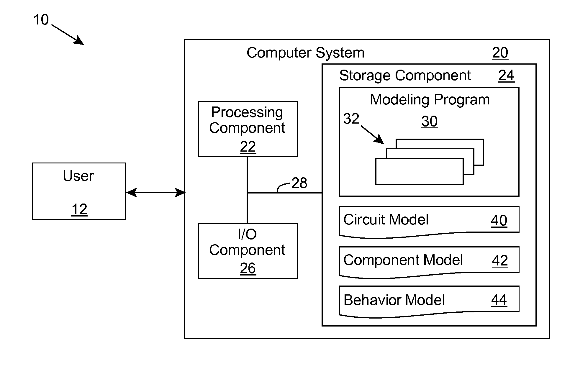
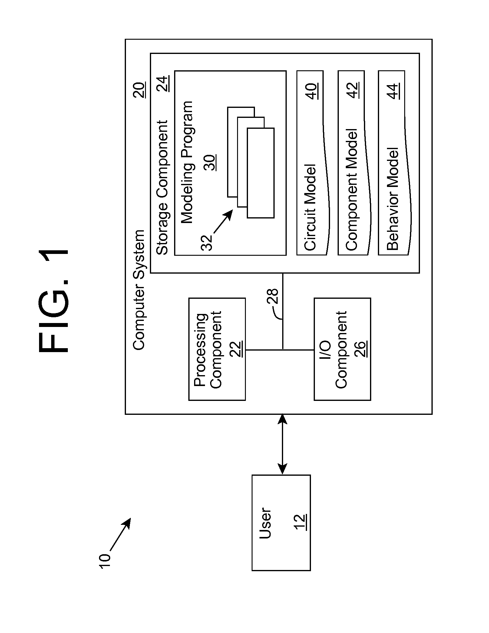
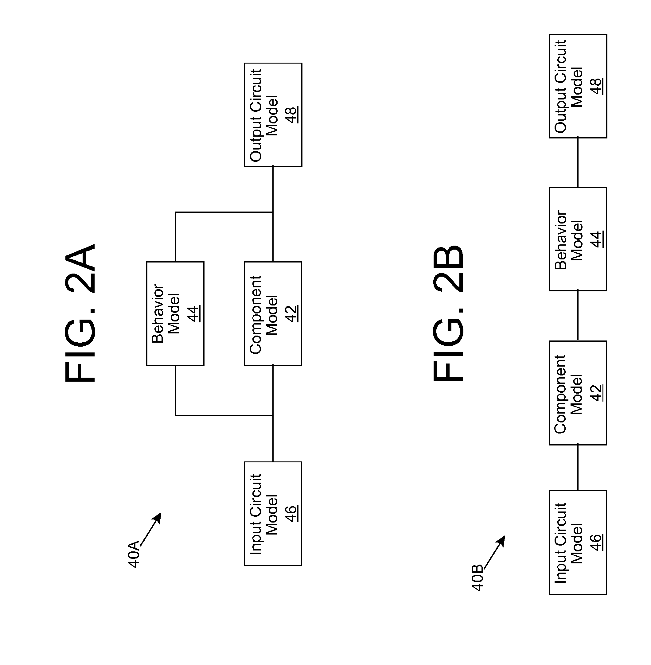
[0021]As indicated above, aspects of the invention provide a behavior model, which is configured to simulate one aspect of the behavior of a component apart from a component model for the component. The behavior model can be included in a circuit model used to simulate operation of a circuit. The circuit model can include a component model for a component and a corresponding behavior model, which is located in parallel or series with the component model. The component model and behavior model can collectively simulate all of the behavior of the component within the circuit. In an embodiment, the behavior model simulates snapback behavior exhibited by the component. As used herein, unless otherwise noted, the term “set” means one or more (i.e., at least one) and the phrase “any solution” means any now known or later developed solution.

[0022]Turning to the drawings, FIG. 1 shows an illustrative environment 10 for modeling a circuit according to an embodiment. Environment 10 includes a...


PUM


Abstract

A behavior model is provided, which is configured to simulate one aspect of the behavior of a component apart from the component model for the component. The behavior model can be included in a circuit model used to simulate operation of a circuit. The circuit model can include a component model for a component and a corresponding behavior model, which is located in parallel or series with the component model. The component model and behavior model can collectively simulate all of the behavior of the component within the circuit. In an embodiment, the behavior model simulates snapback behavior exhibited by the component.

Description

TECHNICAL FIELD[0001]The disclosure relates generally to circuit models (e.g., design structures), and more particularly, to a plug in model for modeling snapback behavior of a circuit component.BACKGROUND ART[0002]Various semiconductor devices, such as reverse bias diodes, field effect transistors (FETs), such as metal-oxide-semiconductor FETs (MOSFETs), and silicon controlled rectifiers (SCR), exhibit a snapback type of behavior in the current-voltage characteristics. The snapback behavior occurs when a sufficient voltage (i.e., a snapback trigger voltage) is applied across the semiconductor device. The voltage can lead to an avalanche generation of the voltage carriers within the device, which triggers a positive feedback mechanism in the device leading to more and more conduction. The voltage across the device drops to a low value due to a very low dynamic resistance. These devices are often used in electrostatic discharge (ESD) protection circuits because of their voltage snapb...

Claims


Application Information

Patent Timeline
Patent Type & Authority Applications(United States)
IPC IPC(8): G06F17/50
CPCG06F17/5036G06F17/5045G06F17/5068G06F17/5022G06F30/367G06F30/30G06F30/33G06F30/39G06F30/3308G06F30/398
Inventor LI, JUNJUNNAYAK, RAHUL
Owner GLOBALFOUNDRIES INC
Learn More