

Solar cell
- Summary
- Abstract
- Description
- Claims
- Application Information
AI Technical Summary
Benefits of technology
Problems solved by technology
Method used
Image

Examples
first embodiment
(Structure of Solar Cell)
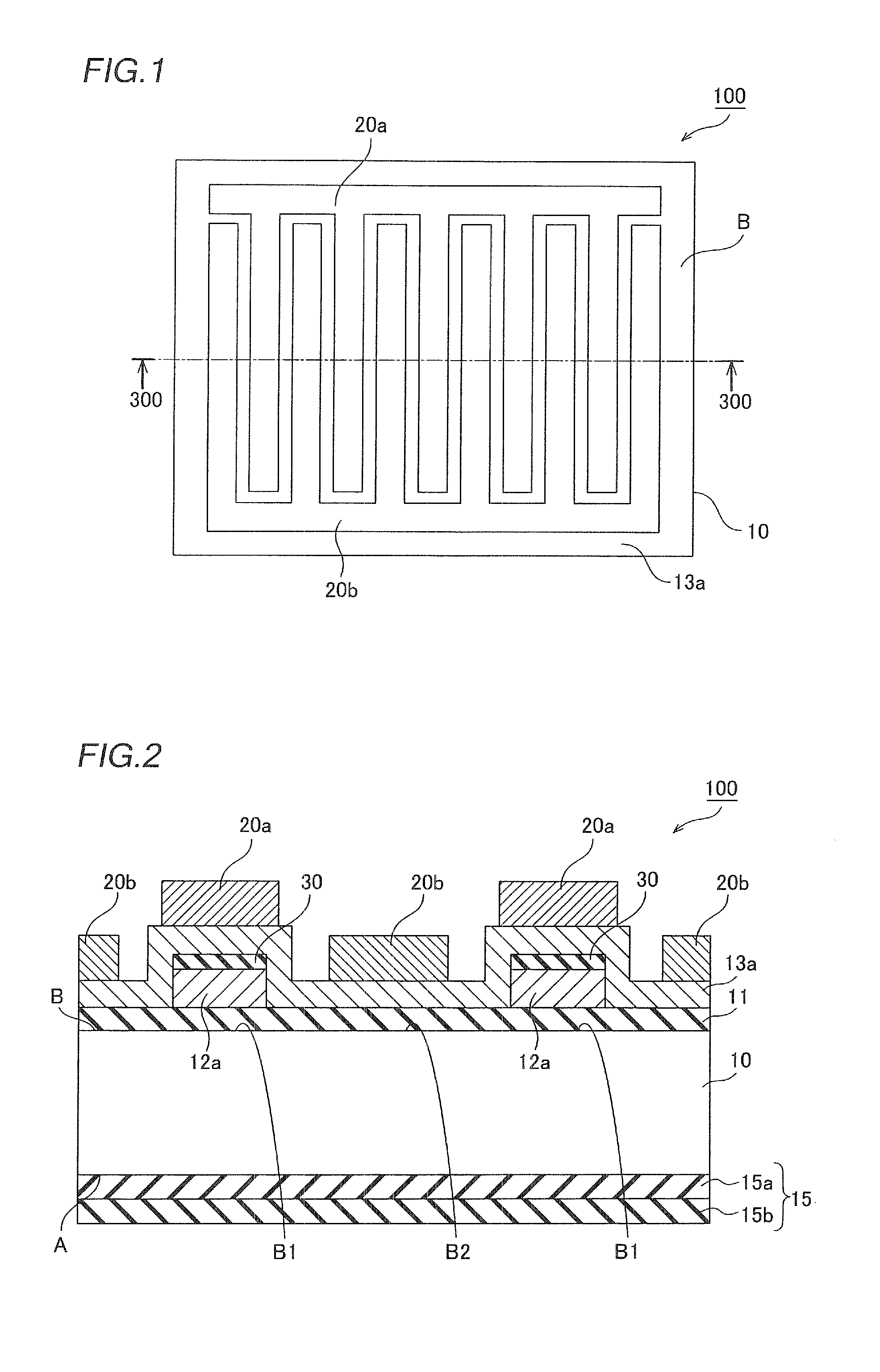
[0026]The structure of a solar cell 100 according to a first embodiment of the present invention is described with reference to FIGS. 1 and 2.
[0027]As shown in FIGS. 1 and 2, the solar cell 100 is provided with a substrate 10 made of a semiconductor. As shown in FIG. 2, the substrate 10 is a semiconductor substrate in the form of a thin plate, and has a p-type or n-type conductivity type. The substrate 10 is made of crystalline silicon such as single-crystalline silicon or polycrystalline silicon, a compound semiconductor such as GaAs or InP, or still another semiconductor which can be formed in a plate shape. The substrate 10 is an example of the “semiconductor substrate” in the present invention.
[0028]The substrate 10 has a photoreceiving surface A and a back surface B. The photoreceiving surface A is a surface upon which light is incident. The back surface B is a surface opposite to the photoreceiving surface A. Both of the photoreceiving surface A and th...
second embodiment
[0057]A solar cell 150 according to a second embodiment of the present invention is now described with reference to FIG. 6.
(Structure of Solar Cell)
[0058]As shown in FIG. 6, a cap layer 31 is formed between the upper surface and the side surfaces of a p-type amorphous semiconductor layer 12a and an n-type amorphous semiconductor layer 13a in the solar cell 150 according to the second embodiment. The remaining structure of the second embodiment is similar to that of the aforementioned first embodiment.
(Method of Manufacturing Solar Cell)
[0059]A method of manufacturing the solar cell 150 according to the second embodiment is now described.
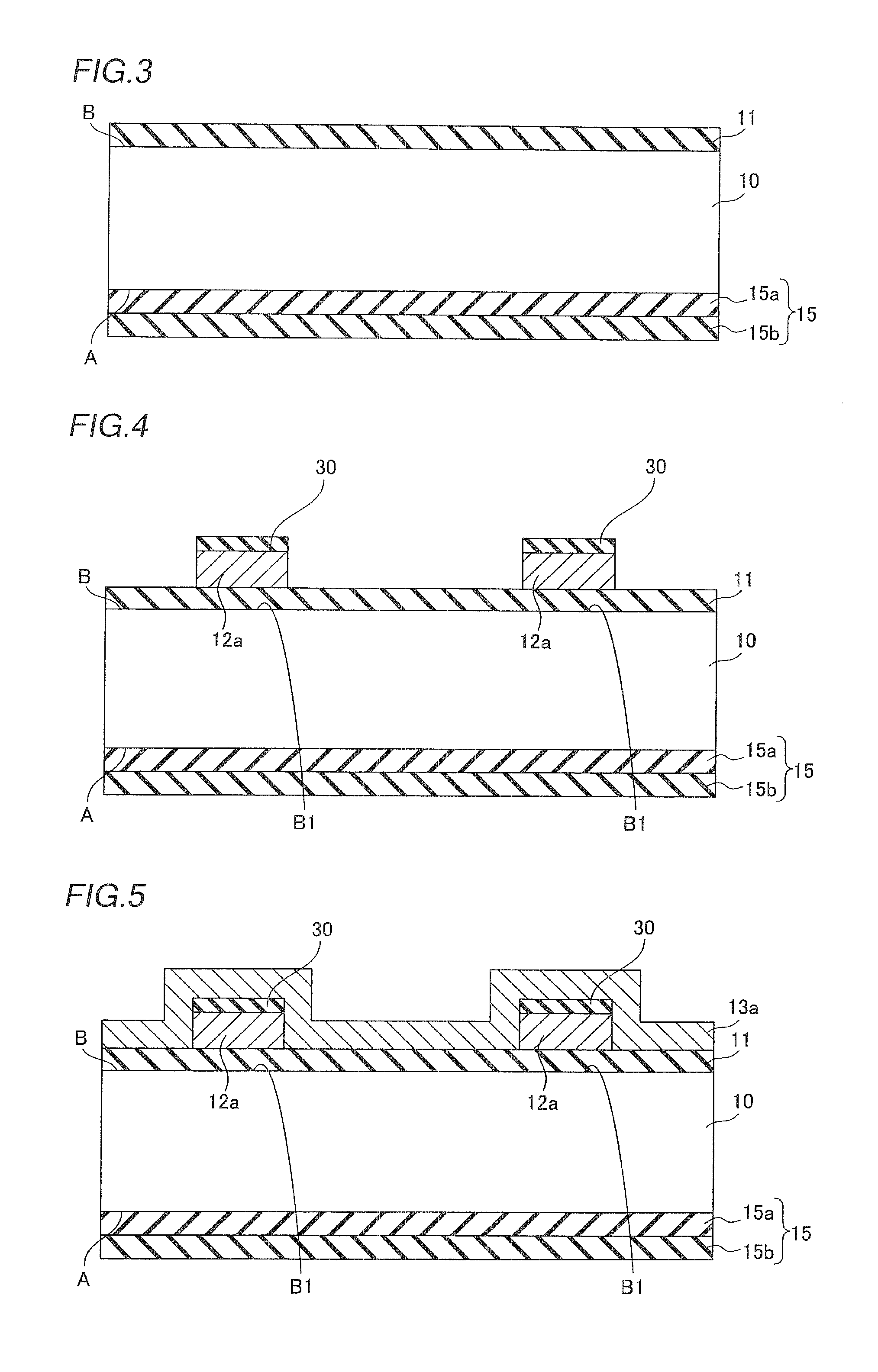
[0060]First, a light incidence-side structure 15 is formed substantially on the whole of a photoreceiving surface A of a substrate 10, similarly to the first embodiment. Further, an i-type amorphous semiconductor layer 11 is formed substantially on the whole of a back surface B of the substrate 10 by CVD. Then, the p-type amorphous semiconductor laye...
third embodiment
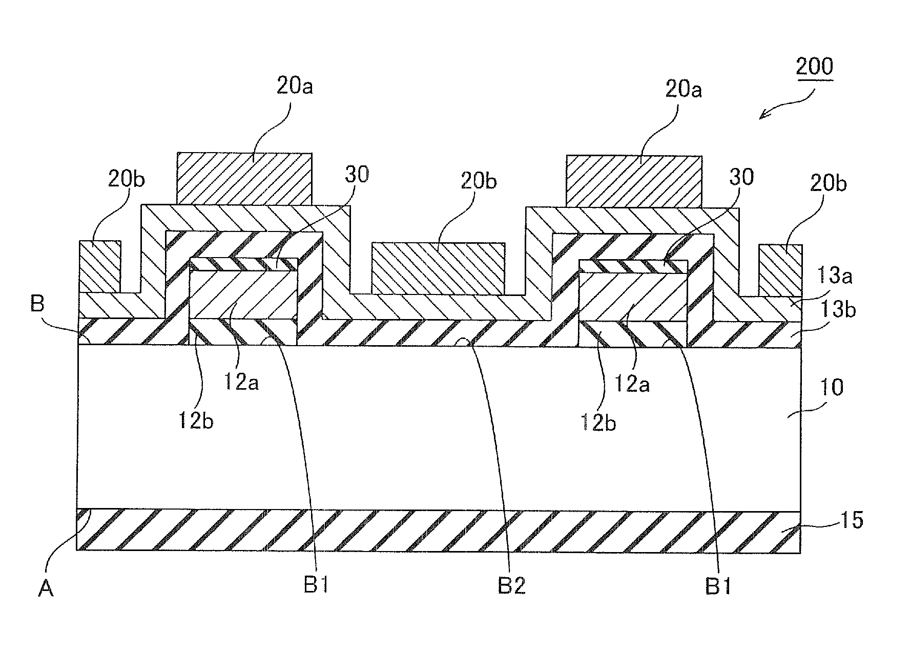
[0064]A solar cell 200 according to a third embodiment of the present invention is now described with reference to FIGS. 7 to 11. In the following, points different from those of the first embodiment are mainly described.
(Structure of Solar Cell)
[0065]FIG. 7 is a sectional view of the solar cell 200 according to the third embodiment of the present invention. As shown in FIG. 7, an i-type amorphous semiconductor layer 12b and a p-type amorphous semiconductor layer 12a are successively stacked on the surface of a first region B1 of a back surface B of a substrate 10. In other words, the i-type amorphous semiconductor layer 12b is formed between the semiconductor substrate 10 and the p-type amorphous semiconductor layer 12a. A cap layer 30 is formed on the upper surface of the p-type amorphous semiconductor layer 12a. An i-type amorphous semiconductor layer 13b and a p-type amorphous semiconductor layer 13a are stacked to extend over the back surface B (a second region B2 adjacent to t...
PUM
 Abstract
Description
Claims
Application Information