SiC single crystal substrate, SiC single crystal epitaxial wafer, and SiC semiconductor device

Active Publication Date: 2010-08-12
DENSO CORP
View PDF33 Cites 20 Cited by
  • Summary
  • Abstract
  • Description
  • Claims
  • Application Information

AI Technical Summary

Benefits of technology

[0016]According to a fifth aspect of the present disclosure, a silicon carbide semiconductor device includes: a field effect transistor as an electric device having a channel surface of a (1-100)-face disposed in the silicon carbide single crystal epitaxial wafer. The device characteristics become much excellent.

Problems solved by technology

However, the patent documents No. 1 and No. 2 do not teach a threading edge dislocation, and thereby, influence of the threading edge dislocation on the device is not clear.
Thus, the threading screw disl

Method used


Image

  • SiC single crystal substrate, SiC single crystal epitaxial wafer, and SiC semiconductor device
  • SiC single crystal substrate, SiC single crystal epitaxial wafer, and SiC semiconductor device
  • SiC single crystal substrate, SiC single crystal epitaxial wafer, and SiC semiconductor device

Examples


Example

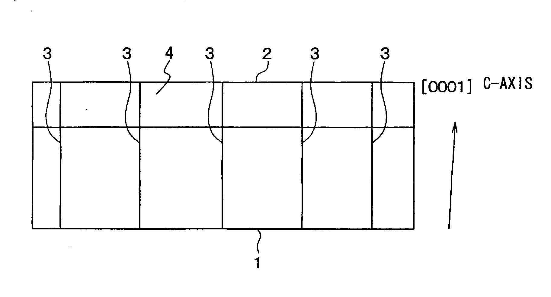
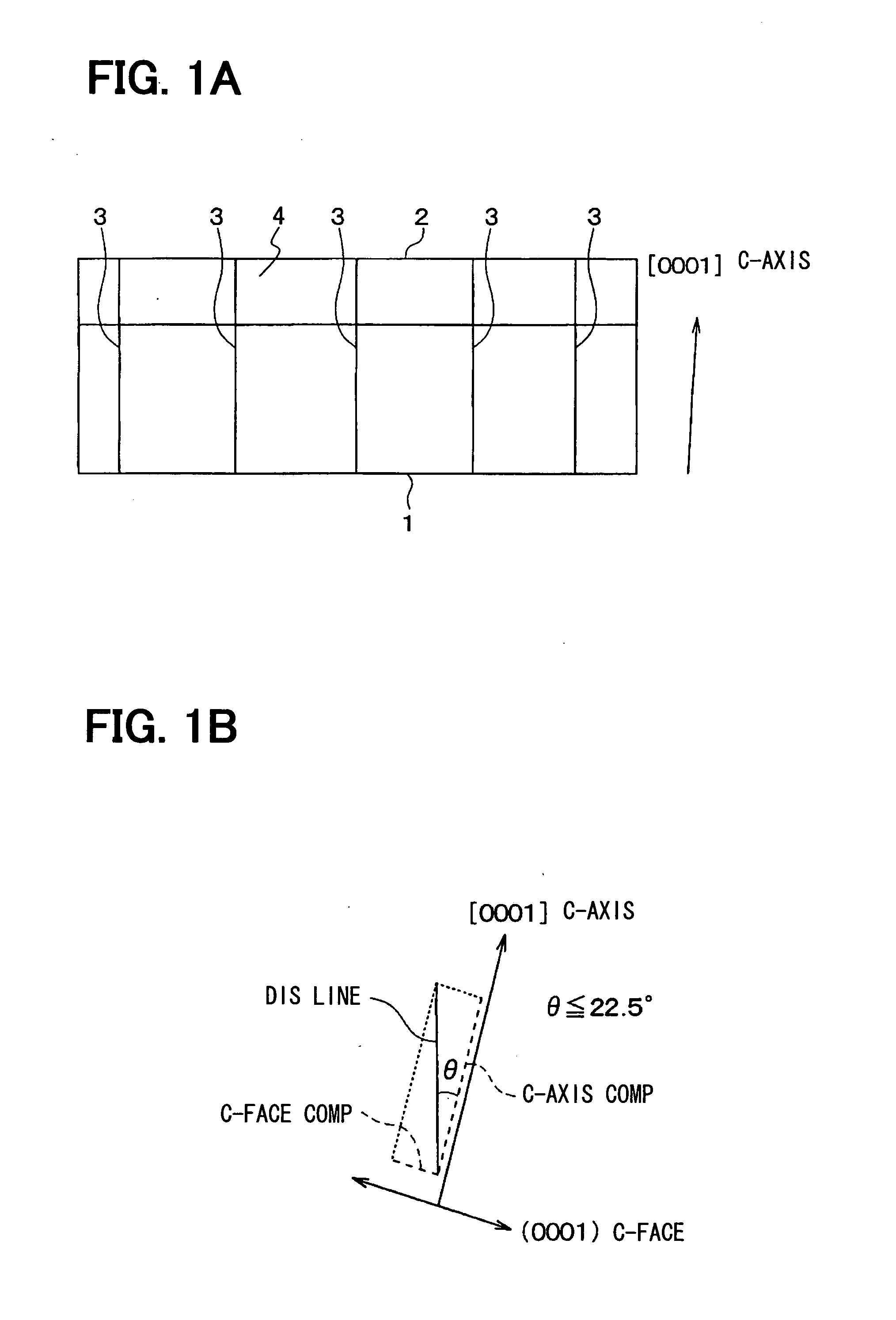
[0040]A first embodiment of the present invention will be explained. FIG. 1A is a cross sectional view of a SiC single crystal epitaxial wafer according to the present embodiment, and FIG. 1B is a vector diagram showing a relationship of an angle between a dislocation line of a threading dislocation in the SiC single crystal epitaxial wafer and a c-axis.

[0041]As shown in FIG. 1A, the SiC single crystal epitaxial wafer is formed such that an epitaxial film 2 is grown on a SiC single crystal substrate 1 made of 4H-SiC. A threading dislocation 3 is disposed in both of the SiC single crystal substrate 1 and the epitaxial film 2. At least the threading dislocation 3 formed in the epitaxial film 2 has an angle θ between a direction of a dislocation line and a [0001]-orientation c-axis equal to or smaller than 22.5 degrees (that is 19.5 degrees plus 3 degrees, i.e., =19.5°+3°). Here, the direction of the dislocation line of the threading dislocation 3 in the SiC single crystal substrate 1 ...

Example

[0043]A second embodiment of the present invention will be explained. The present embodiment provides to align the direction of the dislocation line of the threading dislocation 3 to be restricted and more specifically, compared with the first embodiment. Here, the structure of the SiC single crystal epitaxial wafer according to the present embodiment is similar to that of the first embodiment. Thus, difference between the present and first embodiments will be explained.

[0044]In the SiC single crystal epitaxial wafer shown in FIG. 1A according to the present embodiment, all of the threading dislocations 3 disposed in the epitaxial film 2 are aligned such that the angle θ between the direction of the dislocation line and the [0001]-orientation c-axis is in a range between minus three degrees and plus three degrees with respect to a specific angle. For example, the specific angle is 19.5 degrees (i.e., the [2-203]-orientation direction) or 17 degrees (i.e., the [11-23]-orientation dir...

Example

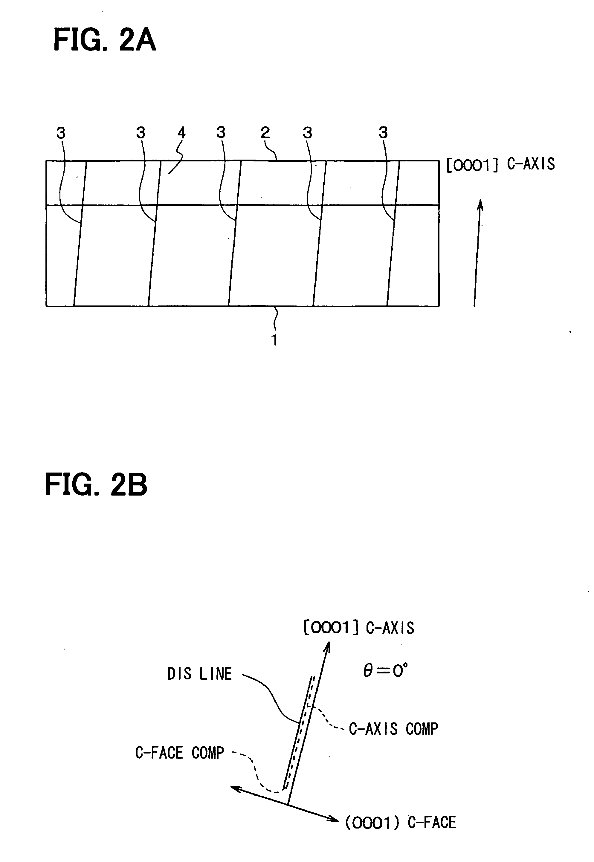
[0046]A third embodiment of the present invention will be explained. The present embodiment provides to align the direction of the dislocation line of the threading dislocation 3 to be restricted and more specifically to the direction of the c-axis as a center, compared with the first embodiment. Here, the structure of the SiC single crystal epitaxial wafer according to the present embodiment is similar to that of the first embodiment. Thus, difference between the present and first embodiments will be explained.

[0047]In the SiC single crystal epitaxial wafer shown in FIG. 1A according to the present embodiment, all of the threading dislocations 3 disposed in the epitaxial film 2 are aligned such that the direction of the dislocation line is in a range between minus three degrees and plus three degrees with respect to the [0001]-orientation c-axis.

[0048]Thus, the direction of the dislocation line of the threading dislocation 3 is aligned to the [0001]-orientation c-axis as a center. ...


PUM

PropertyMeasurementUnit
Angleaaaaaaaaaa
Angleaaaaaaaaaa
Angleaaaaaaaaaa

Abstract

A direction of a dislocation line of a threading dislocation is aligned, and an angle between the direction of the dislocation line of the threading dislocation and a [0001]-orientation c-axis is equal to or smaller than 22.5 degrees. The threading dislocation having the dislocation line along with the [0001]-orientation c-axis is perpendicular to a direction of a dislocation line of a basal plane dislocation. Accordingly, the dislocation does not provide an extended dislocation on the c-face, so that a stacking fault is not generated. Thus, when an electric device is formed in a SiC single crystal substrate having the direction of the dislocation line of the threading dislocation, which is the [0001]-orientation c-axis, a SiC semiconductor device is obtained such that device characteristics are excellent without deterioration, and a manufacturing yield ration is improved.

Description

CROSS REFERENCE TO RELATED APPLICATION[0001]This application is based on Japanese Patent Application No. 2009-29825 filed on Feb. 12, 2009, the disclosure of which is incorporated herein by reference.FIELD OF THE INVENTION[0002]The present invention relates to a SiC single crystal substrate, a SiC single crystal epitaxial wafer and a SiC semiconductor device.BACKGROUND OF THE INVENTION[0003]Conventionally, a SiC single crystal wafer having high quality is disclosed in the patent documents No. 1 and No. 2. The SiC single crystal wafer, disclosed in the patent documents No. 1 and No. 2 is suitably used for processing a device under a condition that a density of dislocations, which negatively affects on device characteristics, is equal to or smaller than a certain value. Here, the dislocation is a crystal defect along with a line. The types of dislocations as an object are a basal plane dislocation disposed on a (0001)-plane face (i.e., C-face) and a threading screw dislocation in para...

Claims


Application Information

Patent Timeline
IPC IPC(8): H01L29/24
CPCC30B25/20C30B29/36H01L21/02378H01L29/1608H01L21/02529H01L21/02609H01L29/045H01L21/02433C23C16/325H01L21/0445
Inventor KITOU, YASUOWATANABE, HIROKINAGAYA, MASANORIYAMAMOTO, KENSAKUOKUNO, EIICHI
Owner DENSO CORP
Why Eureka
Try Eureka