Circuit structure for a capacitive touch panel

Active Publication Date: 2012-01-19
TPK TOUCH SOLUTIONS (XIAMEN) INC
View PDF5 Cites 7 Cited by
  • Summary
  • Abstract
  • Description
  • Claims
  • Application Information

AI Technical Summary

Benefits of technology

[0007]The main object of the present invention is to provide a circuit structure

Problems solved by technology

However, the impedances of the circuit structures in the prior a

Method used


Image

  • Circuit structure for a capacitive touch panel
  • Circuit structure for a capacitive touch panel
  • Circuit structure for a capacitive touch panel

Examples


Example

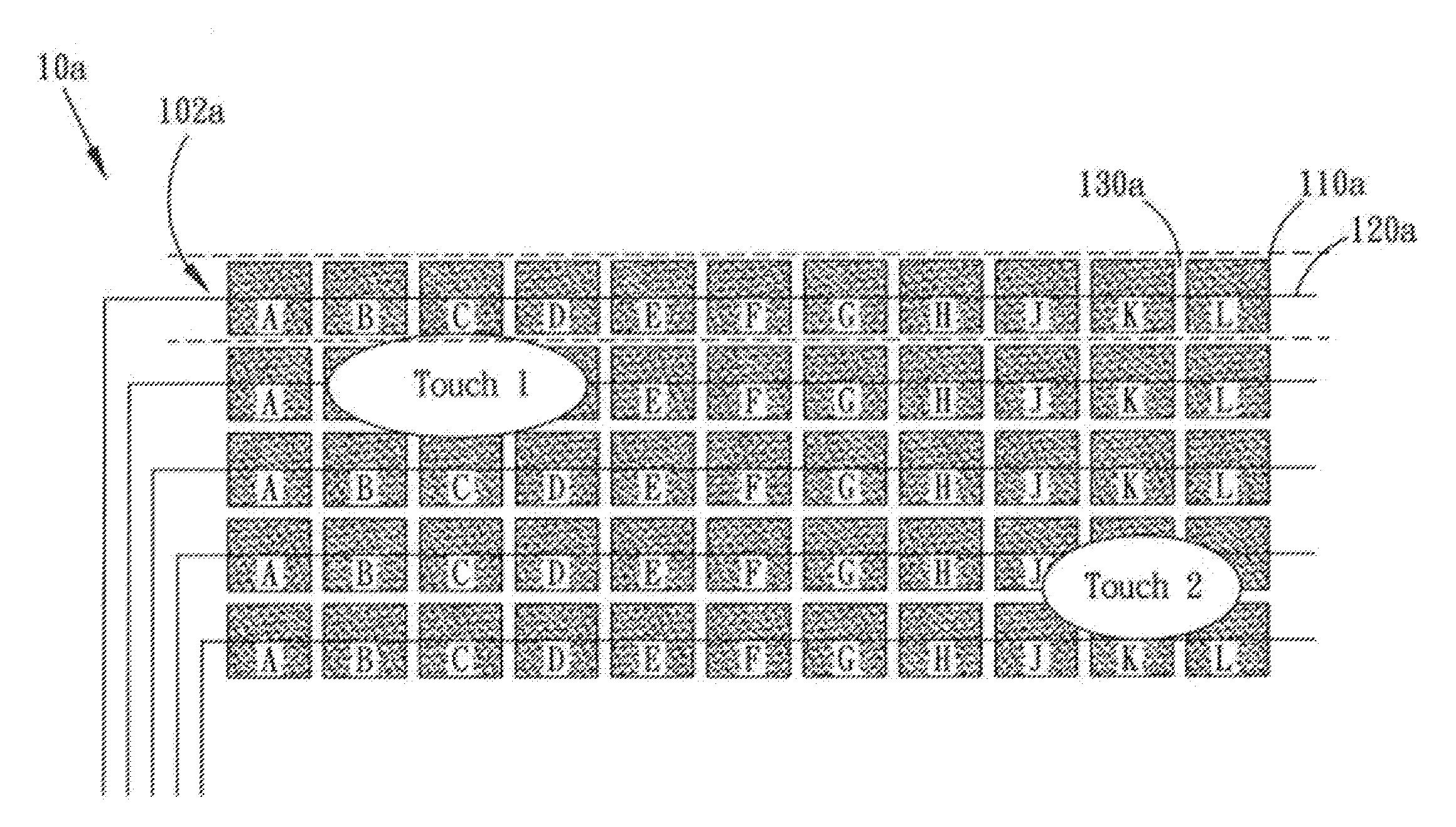
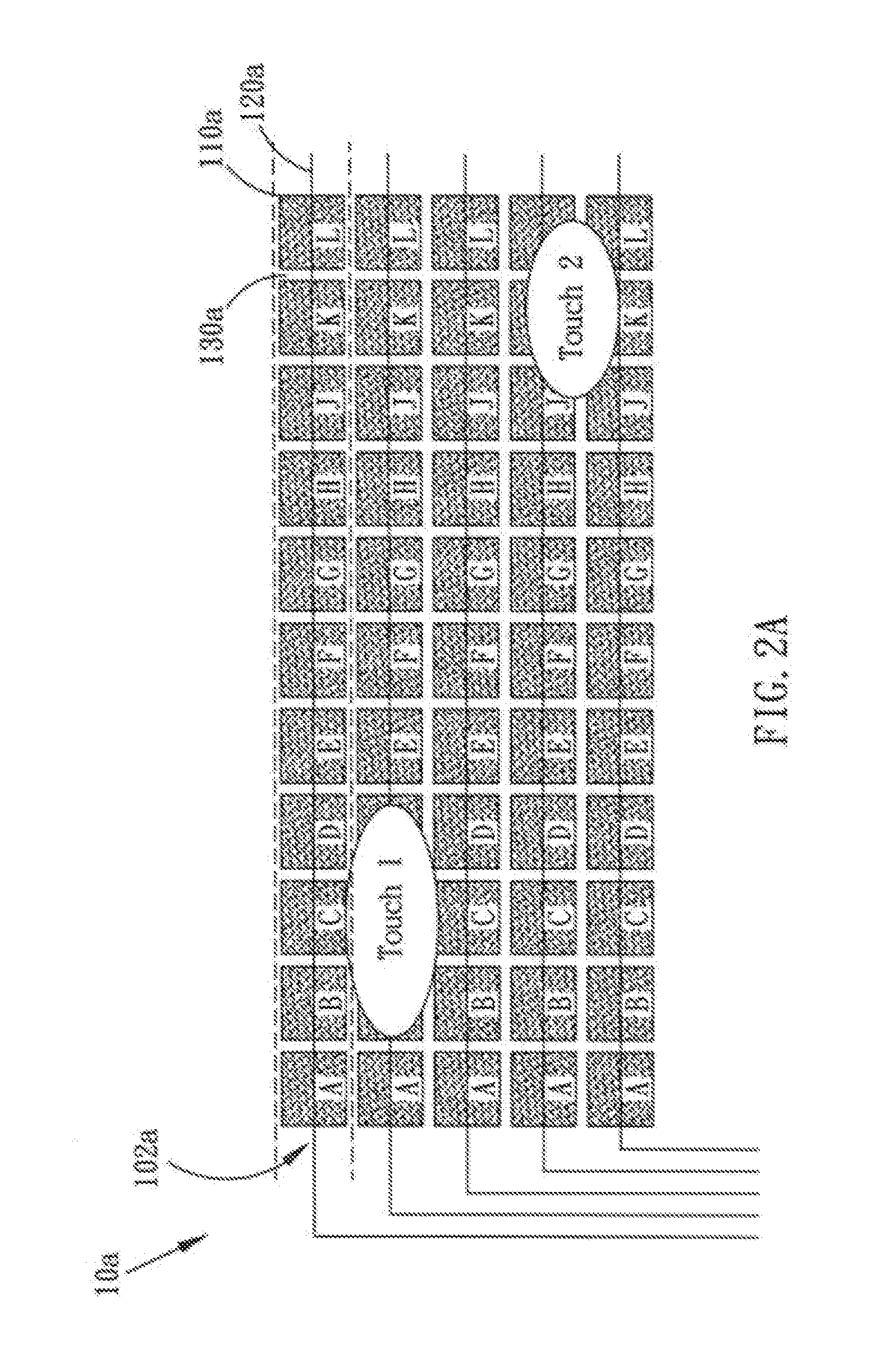
[0017]FIG. 2A is a view showing that the first embodiment of the capacitive touch panel in the present invention. As shown in FIG. 2A, the circuit structure 10a of the capacitive touch panel includes at least one sensing electrode group 102a. Each of the sensing electrode groups 102a includes several electrode sensing blocks 110a and a low impedance metal lead 120a. Each of the electrode sensing blocks 110a includes the same surface area. The sensing electrode blocks 110a are electrically isolated to each other and each of the sensing electrode blocks 110a is electrically connected to the metal lead 120a. There are several intervals 130a with the same distance in the circuit structure 10a and each of the intervals is disposed between the electrode sensing blocks 110a. By cutting the circuit structure of the conventional capacitive touch panel to be several electrode sensing blocks, a low impedance metal lead 120a is then used to connect with each of the electrode sensing block 110a ...

Example

[0019]FIG. 3A is a view showing the second embodiment of the capacitive touch panel in the present invention. As shown in FIG. 3A, the capacitive touch panel 10b in the present embodiment also includes at least one electrode sensing group 102b. Each of the electrode sensing groups 102b includes several electrode sensing blocks 110b and at least one low impedance metal lead 120b. Each of the electrode sensing blocks 110b includes the different surface area. The low impedance metal lead 120b is stacked over and connected to the electrode sensing blocks 110b in parallel. The electrode sensing blocks 110b are arranged in accordance with an arithmetic progression or a geometric progression. There are several intervals 130b with the same distance in the circuit structure 10b and each of the intervals 130b is also disposed between the electrode sensing blocks 110b. When touch 1 and touch 2 are touching on the electrode sensing blocks 110b, a capacitive touching signal will be generated in ...

Example

[0021]FIG. 4A is the third embodiment of the capacitive touch panel in the present invention. The circuit structure 10c in the capacitive touch panel of the present embodiment also includes at least one electrode sensing group 102c. Each of the electrode sensing group 102c includes several electrode sensing blocks 110c, a low impedance metal lead 120c and several intervals 130c disposed between the electrode sensing blocks 110c. The electrode sensing block 110c and the low impedance metal lead 120c are stacked together and connected in parallel. By cutting the circuit structure of the capacitive touch panel to be several electrode sensing blocks 110c, the characteristic of the low impedance metal lead 120c and the layout of stacking the electrode sensing block 110c and the low impedance metal lead 120c are used to reduce the signal transmitting impedance so as to enhance the transmitting efficiency of the capacitive sensing signal. By comparing with the first embodiment and the seco...


PUM


Abstract

A circuit structure for capacitive touch panel is disclosed herein. The circuit structure for capacitive touch panel includes a plurality of metal leads and a plurality of electrode sensing blocks. Those electrode sensing blocks are isolated to each other and electrically connected to the metal leads. The electrode sensing blocks will output a plurality of capacitive signals in accordance with a plurality of touch positions. According to the electrode pattern structure described above, the impedance of the electrode structure can be decreased and the efficiency of the signal transmission can be improved and the sensibility of the touch panel can be increased.

Description

BACKGROUND OF THE INVENTION[0001]1. Field of the Invention[0002]The present invention is related to a circuit structure for a capacitive touch panel, and more particularly is related to a circuit structure for a capacitive touch panel used to reduce the impedance of the circuit structure in the capacitive touch panel.[0003]2. Description of the Prior Art[0004]In recent years, the utilization of the capacitive touch panel is more and more popular, and it may replace the mouse in the future. The user doesn't need to spend too much time in learning how to use the mouse, and the fingers are used to replace the keyboard, the mouse and the touch pen, so that the user can instinctively and simply browse the interne, check email or operate other application software.[0005]The conventional capacitive touch panel is coating a circuit structure, such as Indium Tim Oxide (ITO) or Antimony Tin Oxide (ATO), on a transparent glass. When the human finger touches on the capacitive touch panel, the h...

Claims


Application Information

Patent Timeline
IPC IPC(8): H03K17/975
CPCG06F3/044G06F3/0443G06F3/0445G06F2203/04103
Inventor LIU, CHEN-YUWANG, CHING-YI
Owner TPK TOUCH SOLUTIONS (XIAMEN) INC
Why Eureka
Try Eureka