Mutual capacitance touch display panel and manufacturing method thereof

Inactive Publication Date: 2017-08-03
TCL CHINA STAR OPTOELECTRONICS TECH CO LTD
View PDF1 Cites 4 Cited by
  • Summary
  • Abstract
  • Description
  • Claims
  • Application Information

AI Technical Summary

Benefits of technology

[0007]An object of the present invention is to provide a mutual capacitance touch display panel, which com

Problems solved by technology

However, due to factors, such as higher technical difficulty and being susceptible to signal interference, the sensitivity of the in-cell touch control is generally poor.
Adva

Method used


Image

  • Mutual capacitance touch display panel and manufacturing method thereof
  • Mutual capacitance touch display panel and manufacturing method thereof
  • Mutual capacitance touch display panel and manufacturing method thereof

Examples


Example

[0038]To further expound the technical solution adopted in the present invention and the advantages thereof, a detailed description is given to a preferred embodiment of the present invention and the attached drawings.

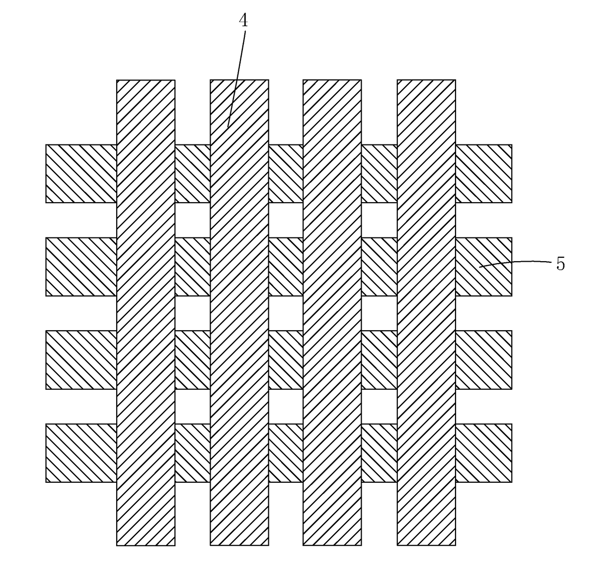
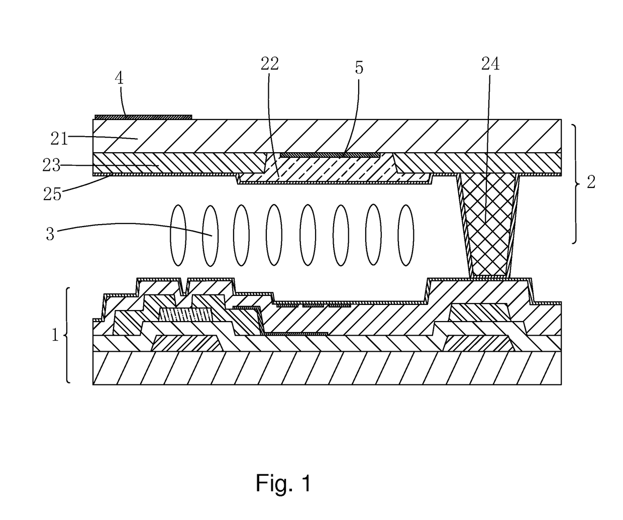
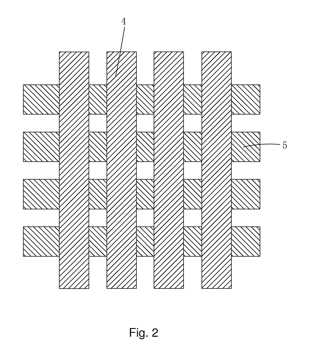
[0039]Referring to both FIGS. 1 and 2, firstly, the present invention provides a mutual capacitance touch display panel, which comprises: a thin-film transistor (TFT) array substrate 1, a color filter (CF) substrate 2 opposite to the TFT array substrate 1, a liquid crystal layer 3 interposed between the TFT array substrate 1 and the CF substrate 2, a plurality of touch transmission electrodes 4 formed on a surface of the CF substrate 2 that is distant from the liquid crystal layer 3 and parallel to each other, and a plurality of transparent touch detection electrodes 5 formed on a surface of the CF substrate 2 that is adjacent to the liquid crystal layer 3 and are parallel to each other and are perpendicular to the touch transmission electrodes 4 in space.

[0040]The TFT...


PUM


Abstract

The present invention provides a mutual capacitance touch display panel and a manufacturing method thereof. The mutual capacitance touch display panel includes touch transmission electrodes (4) that are integrated on a surface of a CF substrate (2) that is distant from a liquid crystal layer (3) and transparent touch detection electrodes (5) integrated on a surface of the CF substrate (2) that is adjacent to the liquid crystal layer (3). The touch detection electrodes (5) are subjected to high temperature annealing treatment. The manufacturing method of the mutual capacitance touch display panel forms, before the formation of the liquid crystal layer (3), the transparent touch detection electrodes (5) on the surface of the CF substrate (2) that is adjacent to the liquid crystal layer (3) and applies high temperature annealing to reduce the impedance of the touch detection electrodes (5), laminates the CF substrate (2) to a TFT base plate (1), and forms, after the formation of the liquid crystal layer (3), the touch transmission electrodes (4) on the surface of the CF substrate (2) that distant from the liquid crystal layer (3). The present invention reduces the impedance of the touch detection electrodes and increases the touch sensitivity of the touch display panel.

Description

BACKGROUND OF THE INVENTION[0001]1. Field of the Invention[0002]The present invention relates to the field of display technology, and in particular to a mutual capacitance touch display panel and a manufacturing method thereof.[0003]2. The Related Arts[0004]With the rapid process of the display technology, touch display panels have been widely accepted and used by people. For example, intelligent phones and tablet computers both involve the use of touch display pane. The touch display panel is formed by applying the embedding touch technology to combine a touch panel and a liquid crystal display panel with each other as a unit with the functionality of the touch panel embedded in the liquid crystal display panel to make the liquid crystal display panel to simultaneously possess the functions of displaying and touch control / input.[0005]The liquid crystal display panels are generally made up of a color filter (CF) substrate, a thin-film transistor (TFT) array substrate, and a liquid c...

Claims


Application Information

Patent Timeline
IPC IPC(8): G06F3/041G02F1/1333G02F1/1339G02F1/1335G02F1/1343G06F3/044G02F1/1368
CPCG06F3/0412G06F3/044G02F1/13338G02F1/1368G02F1/133514G06F2203/04104G02F1/134309G02F1/133512G02F1/13394G02F1/133516G06F2203/04103G02F1/13439G06F3/0445G06F3/0446
Inventor XU, XIANGYANG
Owner TCL CHINA STAR OPTOELECTRONICS TECH CO LTD
Why Eureka
Try Eureka