Thin circuit board

Inactive Publication Date: 2007-06-07
PHOENIX PRECISION TECH CORP
View PDF7 Cites 7 Cited by
  • Summary
  • Abstract
  • Description
  • Claims
  • Application Information

AI Technical Summary

Benefits of technology

[0015] In addition, by eliminating the need of plated through holes, the length of the conductive path is reduced. Also, parasitic capacitance and inductance introduced by plated through holes are eliminated. As a result, the impedance of the thin circuit board is reduced and the electrical performance of the thin circuit board is enhanced. Therefore, the thin circuit board of the present invention is suitable to be applied to high frequency and high speed electronic products.
[0016]

Problems solved by technology

In addition, to form through holes in the core board, high cost drilling machines are needed, thereby increasing the fabrication cost.
To form through holes by mechanical drilling, fine drilling bits are needed, which are easy to wear out and accordingly need to be changed periodically, thereby increasing the material cost.
On the other hand, it is difficult to drill through the core board by laser drilling, especially to drill through the core board having multiple metal layers.
Moreover, to effectively form conductive

Method used


Image

  • Thin circuit board
  • Thin circuit board
  • Thin circuit board

Examples


Example

First Embodiment

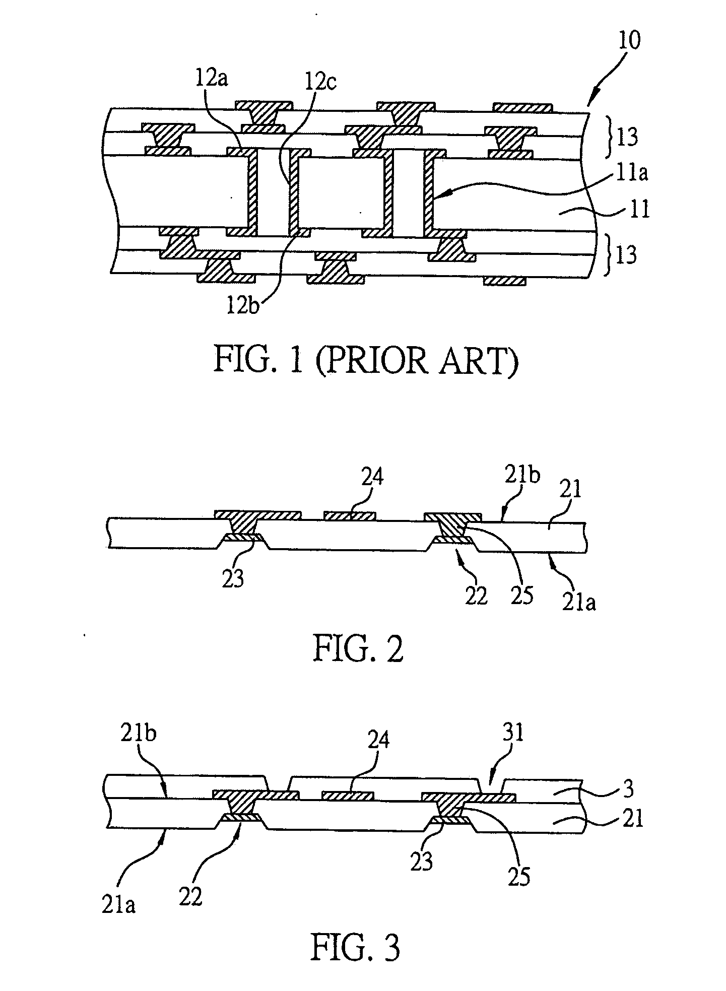
[0026]FIG. 3 shows structure of a thin circuit board according to a first embodiment of the present invention. As shown in FIG. 3, a solder mask layer 3 is formed on the surface 21b of the dielectric layer 21 where the circuit layer 24 is formed so as to cover the dielectric layer 21 and the circuit layer 24. A plurality of openings 31 is formed in the solder mask layer 3 to partially expose the circuit layer 24. A solder mask layer (not shown) can also be formed on the surface 21a of the dielectric layer 21 where the cavity 22 is formed, the solder mask layer having openings to expose the metal pad 23. As a result, a double-sided thin circuit board is formed, which can be used as a package substrate in FCBGA (flip chip ball grid array) package, FCCSP (flip chip chip-scale package), PBGA (plastic ball grid array) package, CSP (chip size package) or used as a printed wiring board (PWB) in electric products.

Example

Second Embodiment

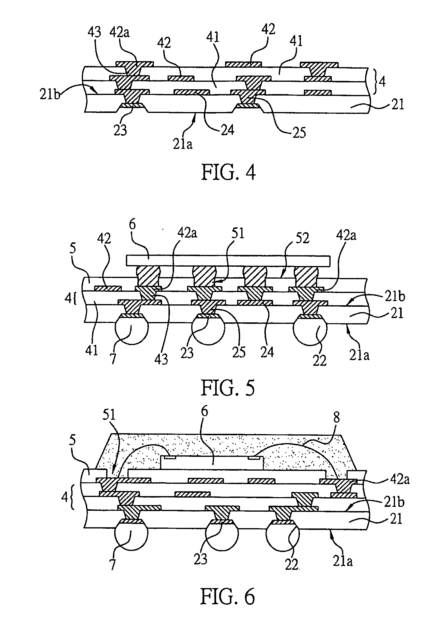
[0027]FIG. 4 shows structure of a thin circuit board according to a second embodiment of the present invention. As shown in FIG. 4, a build-up circuit structure 4 is formed on the surface 21b of the dielectric layer 21 where the circuit layer 24 is formed. The build-up circuit structure 4 includes at least one dielectric layer 41; a circuit layer 42 with a plurality of connecting pads 42a formed on the surface of the dielectric layer 41; and a plurality of conductive vias 43 formed in the dielectric layer 41 and electrically connected with the circuit layer 42, thereby forming a multi-layer circuit board. The multi-layer circuit board can be used as a package substrate as mentioned in the first embodiment or used as a printed wiring board in electric products.

Example

Third Embodiment

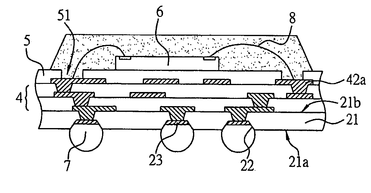
[0028]FIG. 5 shows a thin circuit board structure, which is used as a package substrate. As shown in FIG. 5, a build-up circuit structure 4 is formed on the surface 21b of the dielectric layer 21 according to the second embodiment and a solder mask layer 5 is formed on the surface of the build-up circuit structure 4. A chip receiving area 52 is formed on the surface of the solder mask layer 5, which has a plurality of openings to expose the connecting pads 42a of the circuit layer 42. A semiconductor device 6 such as a chip or a passive component can be disposed on the chip receiving area 52 and electrically connected with the build-up circuit structure 4 through the connecting pads 42a, thereby forming a flip chip structure. Also, a conductive element 7 such as a solder ball, a conductive bump or a pin can be formed in the cavity 22 of the dielectric layer 21 and bonded to surface of the metal pad 23.

[0029] By using the conductive vias 25 to electrically connect t...


PUM


Abstract

A thin circuit board includes a dielectric layer with at least one cavity formed on a surface thereof; a metal pad formed in the cavity; at least one circuit layer formed on another surface of the dielectric layer; and a plurality of conductive vias formed in the dielectric layer to electrically connect the circuit layer to the metal pad. A build-up circuit structure is formed on the surface of the dielectric layer where the circuit layer is formed, and a conductive element is formed on a surface of the metal pad, so as to form a single-sided build-up circuit structure that prevents the use of a core board. Therefore, the thickness of the circuit board can be reduced and the impedance of the circuit board can also be reduced due to elimination of the use of plated through holes.

Description

FIELD OF THE INVENTION [0001] The present invention relates to thin circuit boards, and more particularly to a thin circuit board without a core board. BACKGROUND OF THE INVENTION [0002] Due to gradually reduced size and integrated multiple functions of electronic products, semiconductor packages are accordingly required high integration and miniaturization such as multi chip module packages that have become the mainstream technology in the market. Accordingly, multilayer circuit boards, on which active and passive components are mounted, also need to be formed with high density wiring patterns and interlayer connections to match high density integrated circuit. [0003]FIG. 1 is a cross-sectional view of a prior art multilayer circuit board. As shown in FIG. 1, first, a plurality of through holes 11a is formed in a core board 11. Then, the core board 11 is plated to form conductive layers on both sides of the core board 11 and inner walls of the through holes 11a. The conductive laye...

Claims


Application Information

Patent Timeline
IPC IPC(8): H05K1/16
CPCH01L23/49816H01L23/49822H01L2924/3011H05K1/113H05K3/3457H05K3/4644H05K2201/09472H05K2201/09563H01L2224/16225H01L2224/48227H01L2224/48228H01L2924/15311H01L2924/30107H01L2924/00
Inventor HSU, SHIH-PING
Owner PHOENIX PRECISION TECH CORP
Why Eureka
Try Eureka