

Semiconductor device
a technology of semiconductor devices and semiconductors, applied in semiconductor devices, semiconductor/solid-state device details, electrical apparatus, etc., can solve problems such as deteriorating transmission characteristics of transmission lines, and achieve the effect of suppressing the transmission characteristic of transmission lines
- Summary
- Abstract
- Description
- Claims
- Application Information
AI Technical Summary
Benefits of technology
Problems solved by technology
Method used
Image

Examples
first embodiment
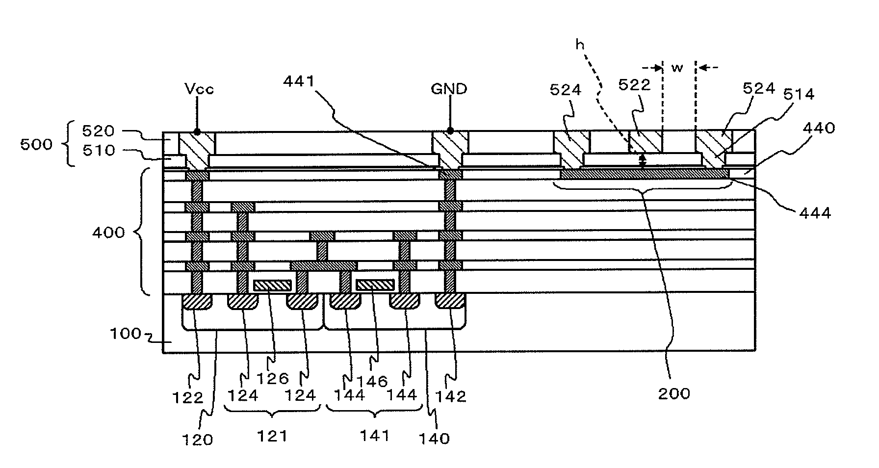
[0031]FIG. 1 is a sectional view illustrating the configuration of a semiconductor device according to the invention. FIG. 14 is an example of a plan view of the semiconductor device shown in FIG. 1. This semiconductor device includes a substrate 100, a first transistor 121, a second transistor 141, a multi-layered interconnect layer 400, a redistribution layer 500, a signal line 522 (the first signal line), a plain line 444, and two coplanar lines 524. The multi-layered interconnect layer 400 and the redistribution layer 500 include three or more interconnect layers in total. The signal line 522 is formed in the a-th layer (a≧2) of the multi-layered interconnect layer 400 and the redistribution layer 500. The plain line 444 is a interconnect line serving as a return path of the signal line 522, is formed in the b-th layer (b400 and the redistribution layer 500, and overlaps with the signal line 522 when seen in a plan view. The two coplanar lines 524 are interconnect lines serving ...
fourth embodiment
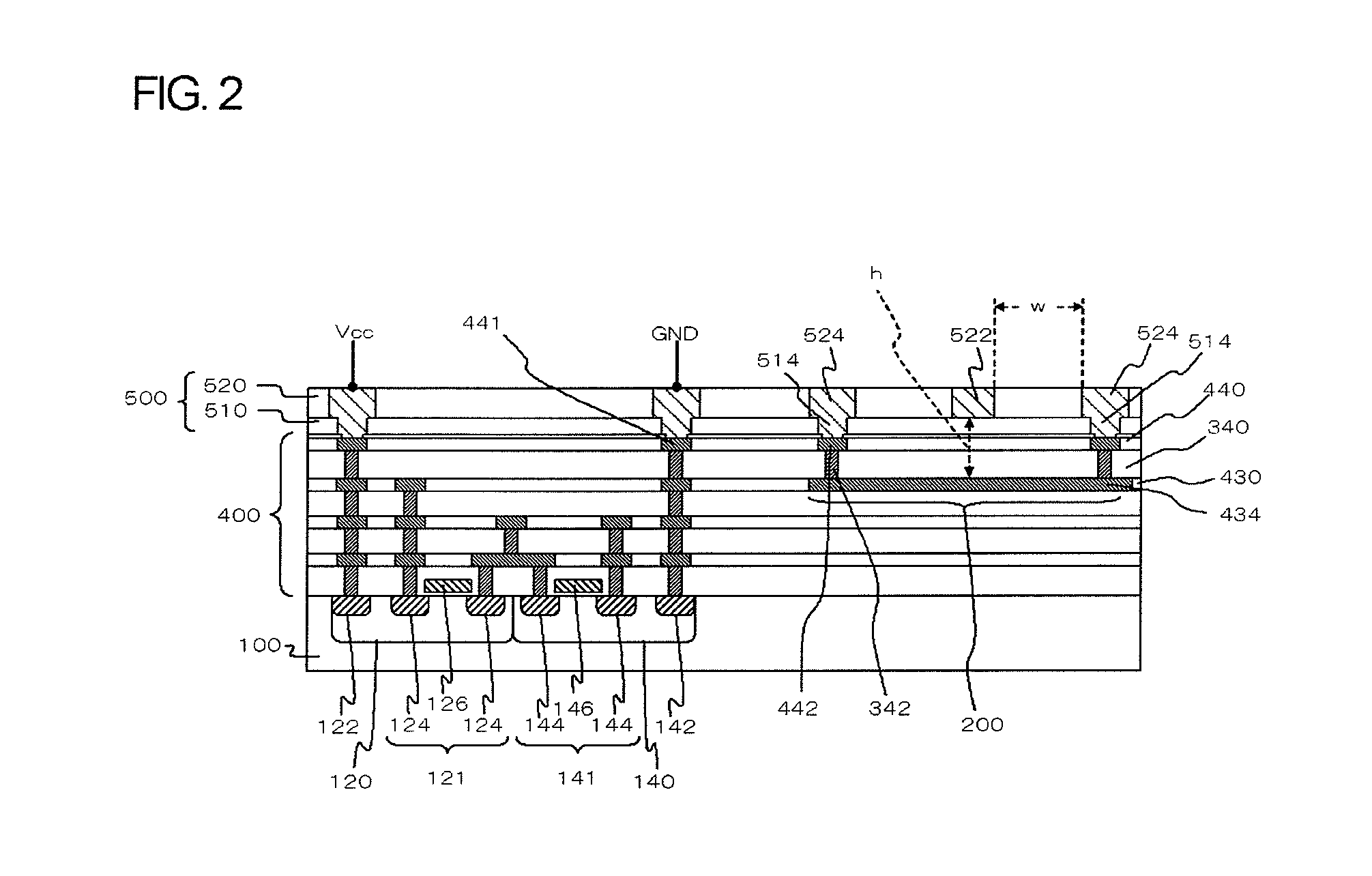
[0055]FIG. 5 is a sectional view illustrating the configuration of a semiconductor device according to the invention. The semiconductor device according to this embodiment has the same configuration as the semiconductor device shown in FIG. 3, except that a plain line 424 is used instead of the plain line 434.
[0056]Specifically, the plain line 424 is formed in the second interconnect layer 420 below the interconnect layer 440 in which the signal line 447 is formed. Two coplanar lines 448 are both connected to the plain line 424 through vias 344, conductor patterns 432, and vias 332. The vias 344 are buried in the insulating interlayer 340 located between the interconnect layer 440 and the interconnect layer 430. The conductor patterns 432 are formed in the interconnect layer 430. The vias 332 are buried in the insulating interlayer 330 located between the interconnect layer 430 and the interconnect layer 420.
[0057]As long as the relational expression h
second embodiment
[0061]The same advantages as described in the second embodiment can be achieved from this embodiment.
[0062]FIG. 7 is a sectional view illustrating the configuration of a semiconductor device according to a sixth embodiment of the invention. The semiconductor device according to this embodiment has the same configuration as the semiconductor device according to the first embodiment, except that plural vias 514 are formed in a single coplanar line 524 when seen in the width direction of the coplanar lines 524. In the examples shown in the drawing, two vias 514 are formed in a single coplanar line 524 when seen in the width direction thereof, but three or more vias may be formed.
[0063]The same advantages as described in the first embodiment can be achieved from this embodiment. Since plural vias 514 are formed when seen in the width direction of the coplanar lines 524, the resistance between the plain line 444 and the coplanar lines 524 can be lowered. Accordingly, it is possible to fu...
PUM
 Abstract
Description
Claims
Application Information