Optimization design method for the chassis structure of an electronic device based on mechanical, electrical and thermal three-field coupling

a technology of mechanical, electrical and thermal coupling, applied in the direction of design optimisation/simulation, instruments, cad techniques, etc., can solve the problems of long design cycle and difficulty in meeting various requirements, and achieve the effect of efficient chassis design

Inactive Publication Date: 2012-01-19
XIDIAN UNIV
View PDF2 Cites 52 Cited by
  • Summary
  • Abstract
  • Description
  • Claims
  • Application Information

AI Technical Summary

Benefits of technology

[0008]The object of the present invention is to solve the problem that the mechanical field, electrical field and thermal field are separated in the design of the current chassis structure of an electronic device, which results in a long design cycle and difficult...

Problems solved by technology

The object of the present invention is to solve the problem that the mechanical field, electrical field and thermal field are separated in the d...

Method used


Image

  • Optimization design method for the chassis structure of an electronic device based on mechanical, electrical and thermal three-field coupling
  • Optimization design method for the chassis structure of an electronic device based on mechanical, electrical and thermal three-field coupling
  • Optimization design method for the chassis structure of an electronic device based on mechanical, electrical and thermal three-field coupling

Examples


Embodiment Construction

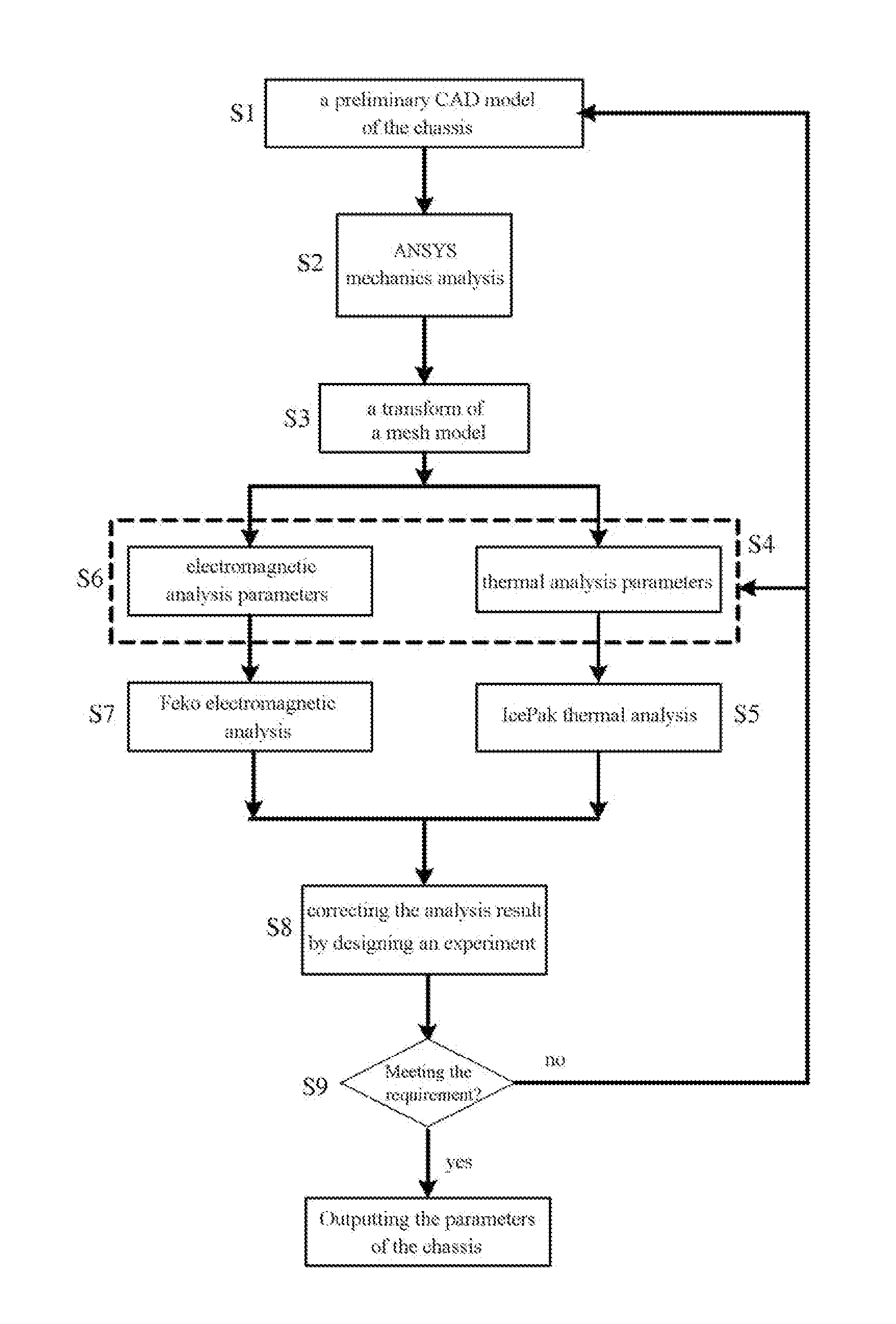
[0052]The present invention is further described in detail with reference to the figures. Refer to FIG. 1, the specific steps of the present invention are as follows:

[0053]Step S1: the preliminary design size of the chassis structure is determined and the preliminary CAD model of the chassis is established.

[0054]According to a work environment of the electronic device and specific requirements, the preliminary design size of the chassis structure is determined, mainly including a material of the chassis, outline sizes such as width a, length l, and height b, a heat dissipation aperture, the number and the position of a fan(s), the size and the position of an internal absorbent material, the position of various major components inside the chassis, a distribution of the internal support structures, and the like, thereby to establish the preliminary CAD model of the chassis for a finite element analysis in mechanics. The determination of the preliminary design size can be based on the ...


PUM


Abstract

An optimizing design method for a chassis structure of electronic equipment is disclosed, including: investigating from the point of view of mechanical, electric and thermal three-field coupling, determining the preliminary design size of the chassis, performing a mechanical analysis by using the software Ansys; converting the mesh model among the three-fields, obtaining the mesh model used for the electromagnetic and thermal analyses; setting the thermal analysis parameters, performing the thermal analysis by using the software IcePak; determining a resonance frequency of the chassis and an electric parameter of the absorbing material, performing an electromagnetic analysis by using the software FeKo; correcting the analysis result by sample testing; determining whether the chassis satisfies the design requirement, if it satisfies the requirement, the optimizing design will be finished, otherwise, modifying the preliminary CAD model, the electromagnetic analysis parameter and the thermal analysis parameter, repeating the above processes until the requirement is satisfied.

Description

TECHNICAL FIELD[0001]The invention relates to the structure design field of an electronic device, in particular to an optimization design method for a structure, which can be used to guide the optimization design for the chassis structure of an electronic device and the analysis of thermal and electromagnetic compatibility property.BACKGROUND[0002]With the rapid development of the electronic industry, the range of application of an electronic device becomes increasingly widely, and an electronic device is present everywhere, not only in a daily life but also in a military field.[0003]An electronic device will be inevitably affected by various external loads such as a vibration, an impact, a centrifugal force and a friction generated from a movement, during the course of transport, storage and use, wherein the vibration and the impact are most harmful. According to statistics, of the environmental factors causing a failure of an airborne electronic device, the vibration factor accoun...

Claims


Application Information

Patent Timeline
IPC IPC(8): G06F17/50G06F17/10
CPCG06F17/5018G06F2217/80G06F2217/16G06F30/23G06F2111/10G06F2119/08
Inventor DUAN, BAOYANQIAO, HUILI, PENGJIANG, SHIBOMA, BOYUANHAN, NINGZENG, LIZHIHE, YU
Owner XIDIAN UNIV
Why Eureka
Try Eureka