Method of manufacturing ceramic electronic component, ceramic electronic component, and wiring board

a technology of electronic components and wiring boards, applied in the direction of sustainable manufacturing/processing, final product manufacturing, printed circuit non-printed electric components association, etc., can solve problems such as the variation in the characteristics of wiring boards embedded with chip capacitors, and achieve the effect of minimizing the variation in characteristics

Active Publication Date: 2012-01-26
MURATA MFG CO LTD
View PDF6 Cites 53 Cited by
  • Summary
  • Abstract
  • Description
  • Claims
  • Application Information

AI Technical Summary

Benefits of technology

[0017]According to various preferred embodiments of the present invention, it is possible to provide a method of manufacturing a ceramic electronic component with minimized variation in characteristics even when embedded in a wiring board, and to provide a ceramic electronic component.

Problems solved by technology

If a chip capacitor is embedded in a wiring board by the method described in the above patent application publication, however, there arises an issue of variation in the characteristics of the wiring board embedded with the chip capacitor.

Method used


Image

  • Method of manufacturing ceramic electronic component, ceramic electronic component, and wiring board
  • Method of manufacturing ceramic electronic component, ceramic electronic component, and wiring board
  • Method of manufacturing ceramic electronic component, ceramic electronic component, and wiring board

Examples


first preferred embodiment

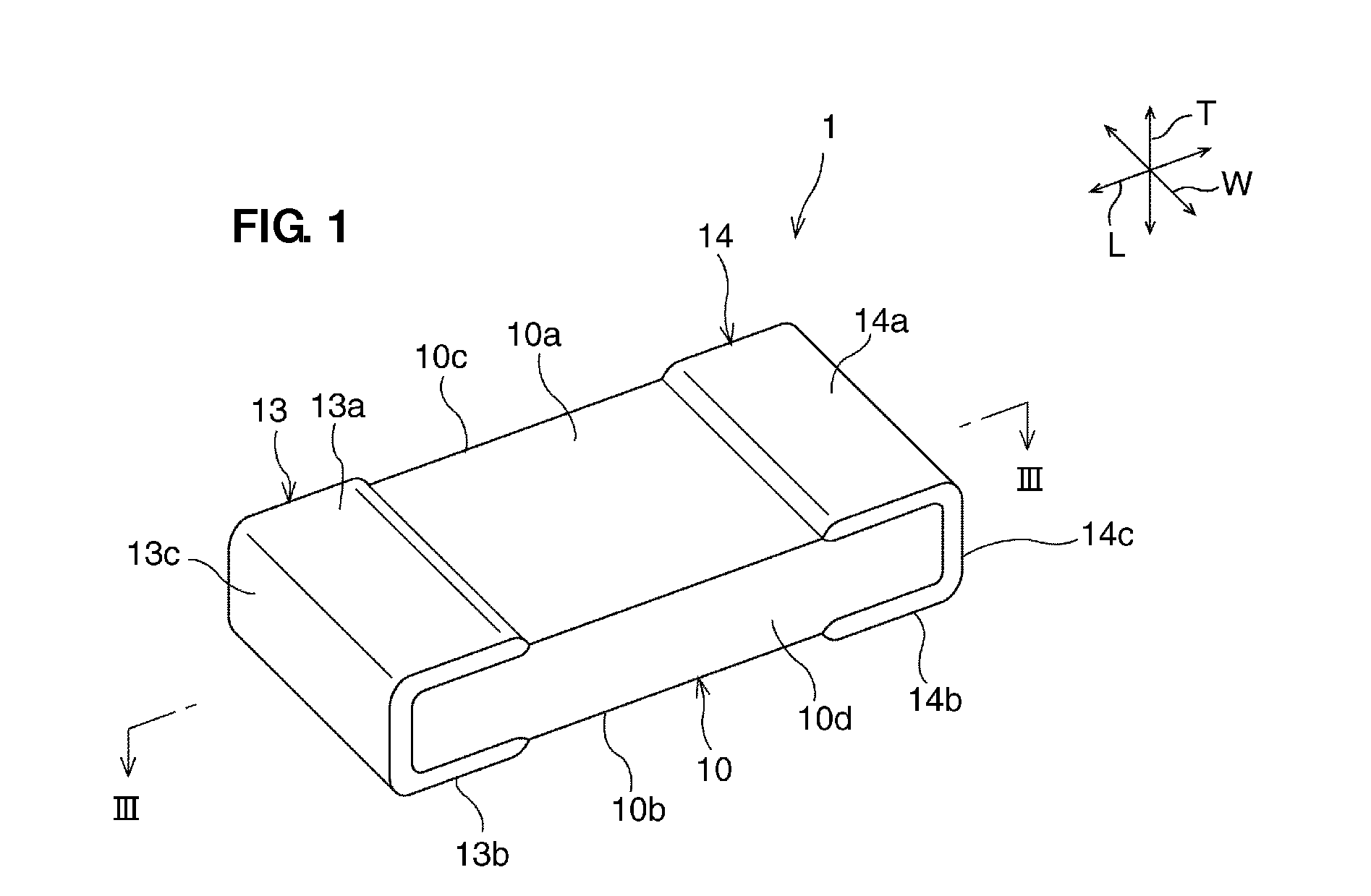
[0036]A first preferred embodiment of the present invention will be described below with reference to a ceramic electronic component 1 illustrated in FIG. 1 as an example. The ceramic electronic component 1, however, is only an example. The present invention is not limited at all by the ceramic electronic component 1 and a manufacturing method thereof described below.

[0037]FIG. 1 is a schematic perspective view of a ceramic electronic component according to a first preferred embodiment.

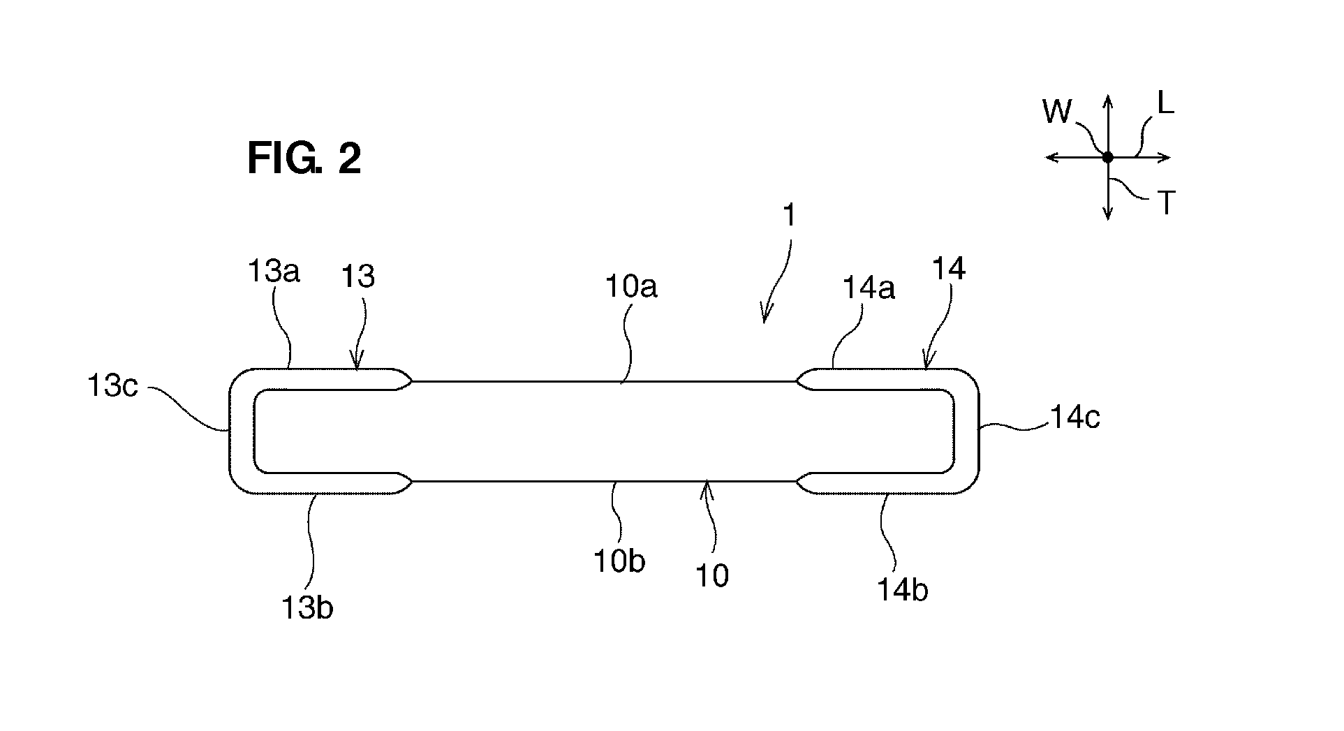
[0038]FIG. 2 is a schematic side view of the ceramic electronic component according to the first preferred embodiment. FIG. 3 is a schematic cross-sectional view of FIG. 1 taken along the line III-III. FIG. 4 is an enlarged schematic cross-sectional view of a portion of the ceramic electronic component according to the first preferred embodiment. FIG. 5 is a schematic cross-sectional view of FIG. 3 taken along the line V-V.

[0039]With reference to FIGS. 1 to 5, the configuration of the ceramic electron...

second preferred embodiment

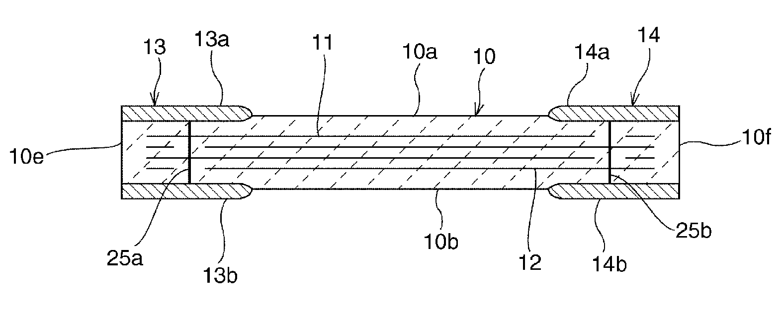
[0096]FIG. 17 is a schematic cross-sectional view of a ceramic electronic component according to a second preferred embodiment of the present invention.

[0097]In the above-described first preferred embodiment, description has been made of the example in which each of the first and second internal electrodes 11 and 12 is drawn to the first or second end surface 10e or 10f, and in which each of the first and second end surfaces 10e and 10f includes the first or second external electrode 13 or 14, to thereby electrically connect each of the first and second internal electrodes 11 and to the first or second external electrode 13 or 14. The present invention, however, is not limited to this configuration.

[0098]For example, as illustrated in FIG. 17, via hole electrodes 25a and 25b may be formed to draw the first and second internal electrodes 11 and 12 to the first and second main surfaces 10a and 10b and electrically connect the first and second internal electrodes 11 and 12 to the first...

experiment examples 1 to 5

[0099]As described in Table 1 given below, 10000 ceramic electronic components serving as ceramic capacitors similar in configuration to the ceramic electronic component 1 of the above-described first preferred embodiment were produced in each of the experiment examples by the manufacturing method described in the above-described first preferred embodiment with different degrees of polymerization of the binder, and were mounted on a wiring board. Then, in the mounting process, the number of ceramic electronic components that failed to be sucked by a suction head of a mounting device (the number of suction failures) was counted. Further, the number of ceramic electronic components cracked or chipped in the mounting process (the number of cracks or chips) was counted. The results are presented in Table 1 given below.

[0100]Further, the shape of the first main surface was measured with the use of a laser displacement meter to measure the distance X1. The results are presented in Table 1...


PUM

PropertyMeasurementUnit
widthaaaaaaaaaa
distanceaaaaaaaaaa
surface roughnessaaaaaaaaaa

Abstract

A method of manufacturing a ceramic electronic component prevents variations in characteristics even when the ceramic electronic component is embedded in a wiring board. Ceramic green sheets containing an organic binder having a degree of polymerization in a range from about 1000 to about 1500 are prepared. A first conductive paste layer is formed on a surface of each of the ceramic green sheets. The ceramic green sheets are laminated to form a raw ceramic laminated body. A second conductive paste layer is formed on a surface of the raw ceramic laminated body. The raw ceramic laminated body formed with the second conductive paste layer is fired.

Description

BACKGROUND OF THE INVENTION[0001]1. Field of the Invention[0002]The present invention relates to a method of manufacturing a ceramic electronic component, a ceramic electronic component, and a wiring board. The present invention particularly relates to a method of manufacturing a ceramic electronic component that is preferably embedded in a wiring board, a ceramic electronic component, and a ceramic electronic component-embedded wiring board embedded with the ceramic electronic component.[0003]2. Description of the Related Art[0004]In recent years, along with the reduction in size and thickness of electronic devices, such as mobile phones and mobile music players, wiring boards mounted on the electronic devices have been reduced in size.[0005]A method of reducing the size of a wiring board is proposed in, for example, Japanese Unexamined Patent Application Publication No. 2001-352141. The method embeds a chip capacitor in a wiring board, forms a through-hole with a laser in a portio...

Claims


Application Information

Patent Timeline
Patent Type & Authority Applications(United States)
IPC IPC(8): H05K1/18H01C7/02H01C7/13
CPCH01C1/14Y10T29/49155H01C7/02H01G2/06H01G4/228H05K1/186H05K3/321H05K2201/10636H05K2201/1003H05K2201/10022H05K2201/10015H05K1/183H05K2201/10439H01G4/1227H01G4/008H01F2027/2809H01F27/2804H01L41/083Y10T29/49124Y10T29/49085Y10T29/49126Y10T29/49144Y10T29/49117H01C7/008Y02P70/50H10N30/50
Inventor SATOSANADA, YUKIONISHISAKA, YASUHIRO
Owner MURATA MFG CO LTD
Why Eureka
Try Eureka