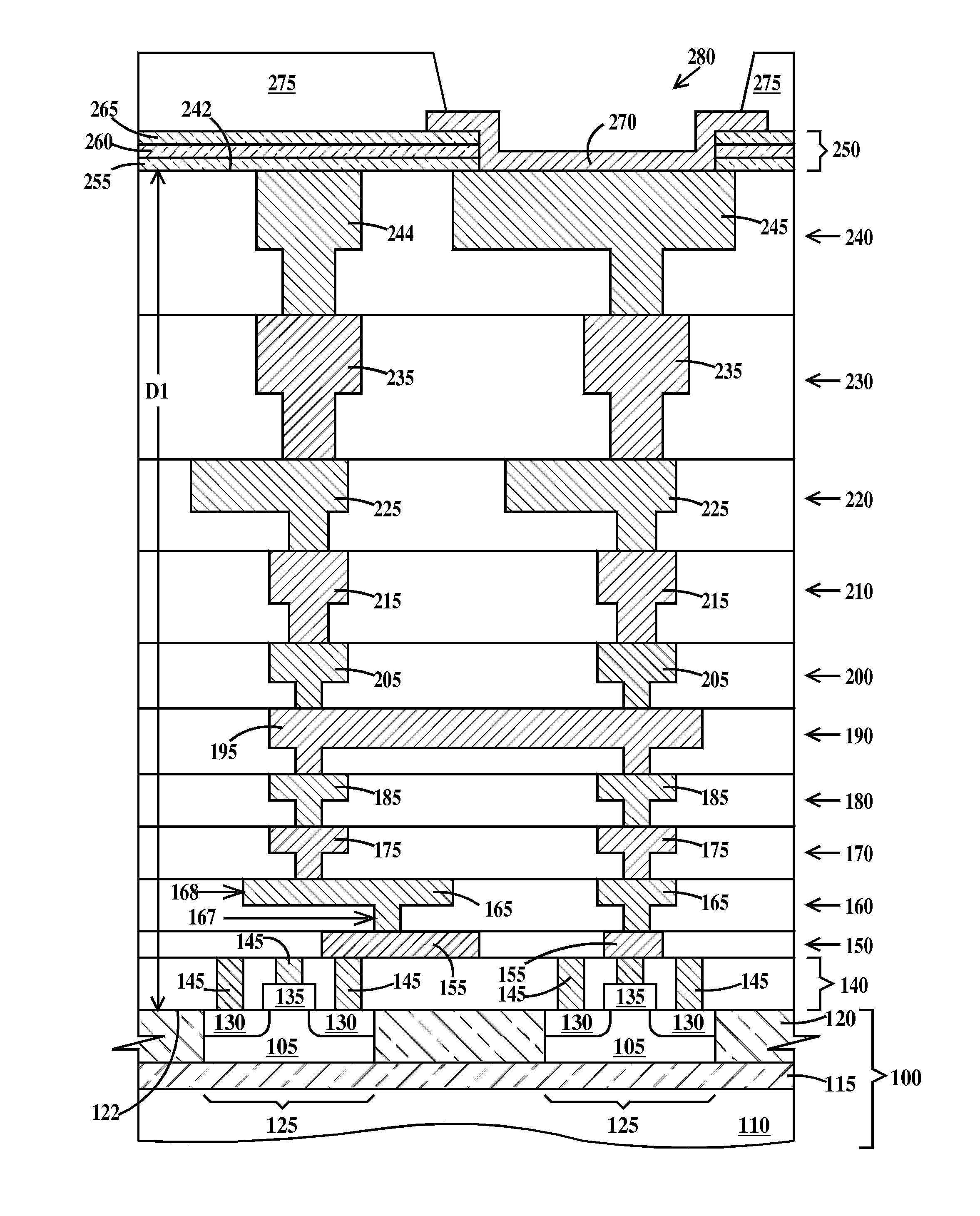
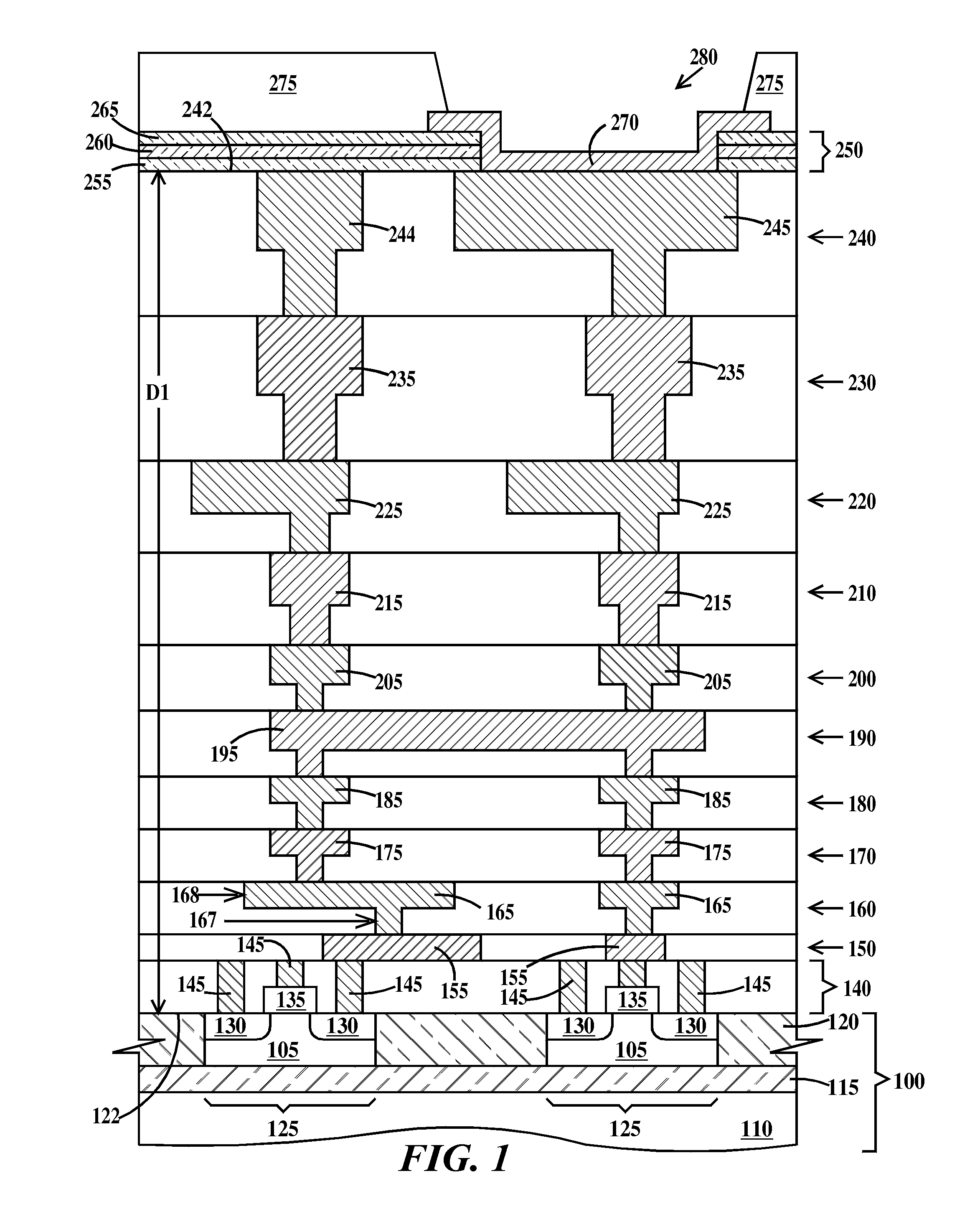
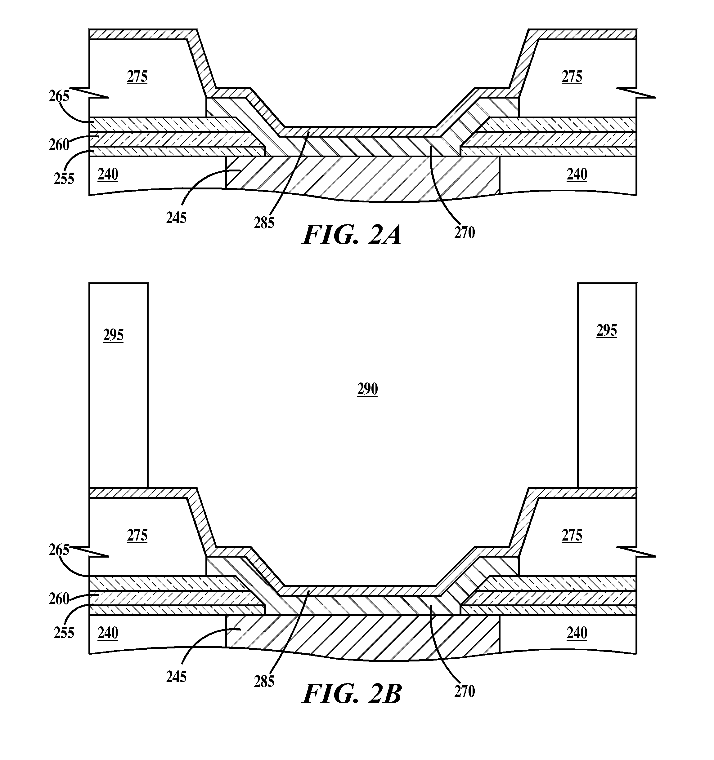
Alpha particle blocking wire structure and method fabricating same

a technology of alpha particle and wire structure, applied in the field of integrated circuits, can solve problems such as failure of integrated circuit chips

Active Publication Date: 2012-02-02
TAIWAN SEMICON MFG CO LTD
View PDF3 Cites 19 Cited by
  • Summary
  • Abstract
  • Description
  • Claims
  • Application Information

AI Technical Summary

Problems solved by technology

The solder may contain isotopes that emit alpha particles

Method used


Image

  • Alpha particle blocking wire structure and method fabricating same
  • Alpha particle blocking wire structure and method fabricating same
  • Alpha particle blocking wire structure and method fabricating same

Examples


Embodiment Construction

[0016]In order for an isotope to cause alpha particle induced soft errors in an integrated circuit chip two conditions must be met. First, the energy of the emitted alpha particles must be high enough to penetrate through intervening materials to the sensitive portions of the integrated circuit chip and low enough to generate sufficient electron hole / pairs in the sensitive portions of the transistors. Second, the alpha particle flux must be high enough so that the probability of sensitive portions of the transistors being hit by the alpha particles is sufficient to cause a detectable rate of fails.

[0017]The solder used in fabricating integrated circuit interconnections may contain 210Pb, which can emit a beta particle and decay to 210Bi. 210Bi can in turn emit a beta particle and decay to 210Po. 210Po in turn can emit a 5.3 MeV alpha particle and decay to 206Pb. It is this alpha particle from 210Po that causes fails in the integrated circuit chip providing the alpha particle can rea...


PUM


Abstract

An alpha particle blocking structure and method of making the structure. The structure includes: a semiconductor substrate; a set of interlevel dielectric layers stacked from a lowermost interlevel dielectric layer closest to the substrate to a uppermost interlevel dielectric layer furthest from the substrate, each interlevel dielectric layer of the set of interlevel dielectric layers including electrically conductive wires, top surfaces of the wires substantially coplanar with top surfaces of corresponding interlevel dielectric layers; an electrically conductive terminal pad contacting a wire pad of the uppermost interlevel dielectric layer; an electrically conductive plating base layer contacting a top surface of the terminal pad; and a copper block on the plating base layer.

Description

FIELD OF THE INVENTION[0001]The present invention relates to the field of integrated circuits; more specifically, it relates to alpha particle blocking wire structures and methods of fabricating alpha particle blocking wire structures.BACKGROUND OF THE INVENTION[0002]It is common practice to connect integrated circuit chips to electronic modules or circuit boards through the use of solders containing lead or a mixture of lead and tin. The solder may contain isotopes that emit alpha particles that can cause failures in the integrated circuit chips. Ceramic and plastic substrates to which integrated circuit chips can be bonded, either using lead solders or other means, can also contain isotopes that emit alpha particles. Since the use of lead and lead / tin solders and ceramic substrates (often used together) is so ubiquitous, improved methods and structures that prevent alpha particles generated in the solder from reaching the alpha particle sensitive regions of the integrated circuit ...

Claims


Application Information

Patent Timeline
IPC IPC(8): H01L21/768H01L23/556
CPCH01L23/3192H01L23/5223H01L2924/00014H01L2224/16225H01L2224/05027H01L23/53238H01L23/556H01L24/03H01L24/05H01L24/06H01L24/11H01L24/13H01L24/14H01L24/16H01L24/73H01L24/81H01L2224/03831H01L2224/0401H01L2224/05558H01L2224/05572H01L2224/05647H01L2224/0603H01L2224/06051H01L2224/10125H01L2224/11462H01L2224/11464H01L2224/13007H01L2224/13028H01L2224/13082H01L2224/13111H01L2224/13116H01L2224/13147H01L2224/13487H01L2224/1403H01L2224/16227H01L2224/73204H01L2224/81447H01L2924/01029H01L2924/01073H01L2924/01082H01L2924/01088H01L2924/01019H01L2924/01033H01L2924/01074H01L2924/01075H01L2924/01084H01L2924/014H01L2224/05552H01L2224/02166H01L2924/14H01L2924/15787H01L2924/00
Inventor CABRAL, JR., CYRILMULLER, K. PAULRODBELL, KENNETH P.
Owner TAIWAN SEMICON MFG CO LTD
Why Eureka
Try Eureka