Equal Potential Ring Structures of Power Semiconductor with Trenched Contact

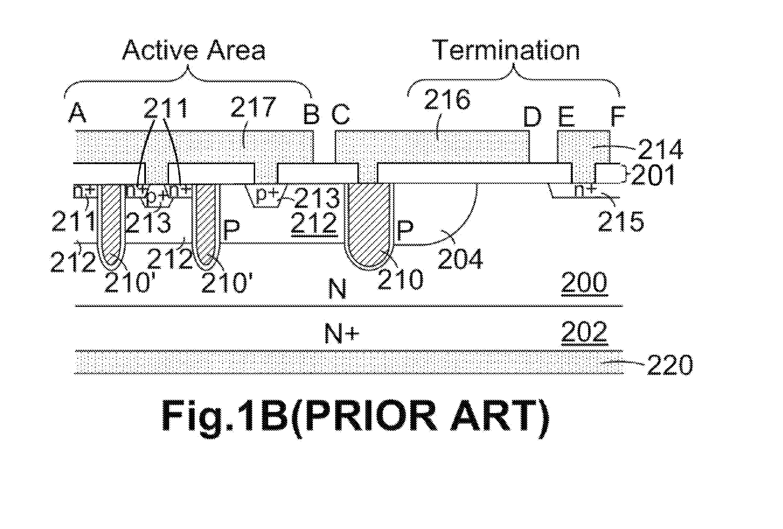
a technology of power semiconductor and ring structure, which is applied in the direction of semiconductor devices, electrical appliances, transistors, etc., can solve the problems of low yield and reliability, affecting the performance of power semiconductor devices, and damage to the front metal of the b>214/b> in fig. 1b, etc., and achieves the effect of easy shrinkag

Inactive Publication Date: 2012-02-16
FORCE MOS TECH CO LTD
View PDF7 Cites 42 Cited by
  • Summary
  • Abstract
  • Description
  • Claims
  • Application Information

AI Technical Summary

Benefits of technology

[0008]The present invention has been conceived to solve the above-described problems with the related art, and it is an object of the invention to provide a semiconductor power device with trenched contact to make the device easily shrunk, and furthermore, to provide a semiconductor power device in which the EPR structure is formed with contact metal plug and penetrating through an insulation layer and further extends downward into an epitaxial layer without having EPR front metal on the top of the contact metal plug so that the pick-up nozzle will not damage the EPR front metal at assembly stage due to the top surface of the contact metal plug is lower than the gate front metal.

Problems solved by technology

Next, as the device size is getting smaller and smaller with increasing of cell density, the EPR front metal 214 in FIG. 1B is often damaged due to touch with gate front metal induced by die pick-up nozzle at assembly stage.
Therefore, the EPR will be easily damaged when the pick-up nozzle touches the EPR front metal, causing EPR shortage with the gate front metal and resulting in low yield and reliability issues as the EPR front metal and the gate front metal have same front metal height.
For other power semiconductor power device, for example N channel trench IGBTs (Insulated Gate Bipolar Transistors) having P+ substrate, the same disadvantage of low yield and reliability issue is also affecting the performance of the power semiconductor device.

Method used


Image

  • Equal Potential Ring Structures of Power Semiconductor with Trenched Contact
  • Equal Potential Ring Structures of Power Semiconductor with Trenched Contact
  • Equal Potential Ring Structures of Power Semiconductor with Trenched Contact

Examples


Embodiment Construction

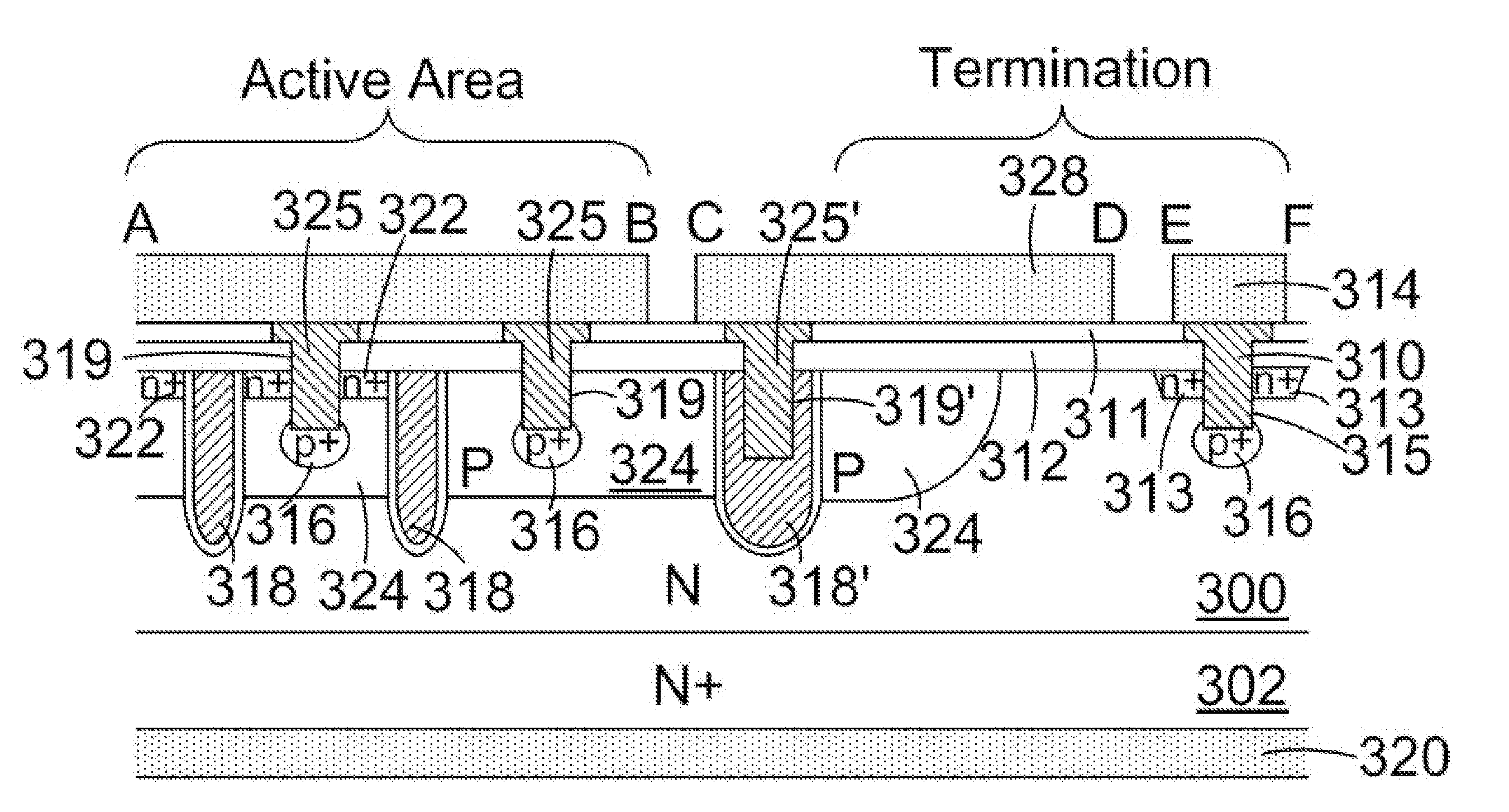
[0030]Please refer to FIG. 3 for cross-sectional view of a trench MOSFET according to the present invention which is also another preferred A-B-C-D-E-F cross section of FIG. 1 where an N-channel trench MOSFET is formed onto an N+ substrate 302 coated with back metal 320 as drain. An active area of the N-channel trench MOSFET comprises: a plurality of first type trenched gate filled with a poly-silicon layer 318 padded by a gate oxide layer in active area; at least a second type trenched gate filled with a poly-silicon layer 318′ padded by a gate oxide layer for gate connection between said active area and termination area, said first type trenched gates and said second type trenched gate are extending into an N epitaxial layer 300 from its top surface; a plurality of source-body trenched contacts 319 having vertical sidewall opened through an insulation layer composed of BPSG 311 and SRO (Silicon Rich Oxide) 312 and an n+ source region 322, and extended into a P body region 324. At ...


PUM


Abstract

A semiconductor power device with trenched contact having improved equal potential ring (EPR) structures for device die size shrinkage and yield enhancement are disclosed. The invented semiconductor power device comprising a termination area including an equal potential ring (EPR) formed with EPR contact metal plug penetrating through an insulation layer covering top surface of epitaxial layer and extended downward into an epitaxial layer. To prevent the semiconductor power device from EPR damage induced by die pick-up nozzle at assembly stage in prior art, some preferred embodiments of the present invention without having EPR front metal.

Description

FIELD OF THE INVENTION[0001]This invention relates generally to a cell structure and device configuration of semiconductor power devices. More particularly, this invention relates to a novel semiconductor power device having equal potential ring structures with trenched contact to further enhanced yield and reliability performance.BACKGROUND OF THE INVENTION[0002]In order to ensure the potential around the device edge has same potential after die sawing for uniform breakdown voltage, an equal potential ring (EPR, similarly hereinafter) is formed in termination area of a semiconductor power device surrounding source front metal and gate front metal, as shown in FIG. 1A. The conventional technologies for implementing the EPR structure of prior art is normally connecting EPR front metal to a source-dopant region by a planar contact on top surface of an epitaxial layer in termination area wherein said source-dopant region is formed simultaneously as source region, as shown in FIG. 1B, w...

Claims


Application Information

Patent Timeline
Patent Type & Authority Applications(United States)
IPC IPC(8): H01L27/082H01L21/768H01L27/088
CPCH01L29/0619H01L29/0638H01L2924/13055H01L2924/13091H01L2224/0603H01L2924/1305H01L29/0623H01L29/1095H01L29/402H01L29/41766H01L29/423H01L29/4236H01L29/456H01L29/7811H01L29/7813H01L29/42372H01L2924/00
Inventor HSHIEH, FWU-IUAN
Owner FORCE MOS TECH CO LTD
Why Eureka
Try Eureka