Light emitting device and method of manufacturing thereof

a technology of light emitting devices and manufacturing methods, which is applied in the manufacturing of semiconductor/solid-state devices, semiconductor devices, electrical devices, etc., can solve the problems of inability to obtain protective films of good quality, and the operation of optical output power decrease, etc., to suppress the discoloration of reflective films and high optical output power

Active Publication Date: 2012-03-01
NICHIA CORP
View PDF3 Cites 23 Cited by
  • Summary
  • Abstract
  • Description
  • Claims
  • Application Information

AI Technical Summary

Benefits of technology

[0011]According to the present invention, a light emitting device capable of maintaining high optical output power while suppressing discoloration of the reflective film and a method of manufacturing thereof may be obtained.

Problems solved by technology

However, when a conventional method is used, there has been a problem that although the optical output power can be improved by the reflective film, decrease in optical output power occurs during the operation.
Therefore, for example, in the vicinity of a light emitting element, the light emitting element itself becomes an obstacle and thus a protective film of good quality has been unable to be obtained.
As a result, deterioration of the reflective film starts to take place from such a portion and which causes discoloration of the reflective film.

Method used


Image

  • Light emitting device and method of manufacturing thereof
  • Light emitting device and method of manufacturing thereof
  • Light emitting device and method of manufacturing thereof

Examples


first embodiment

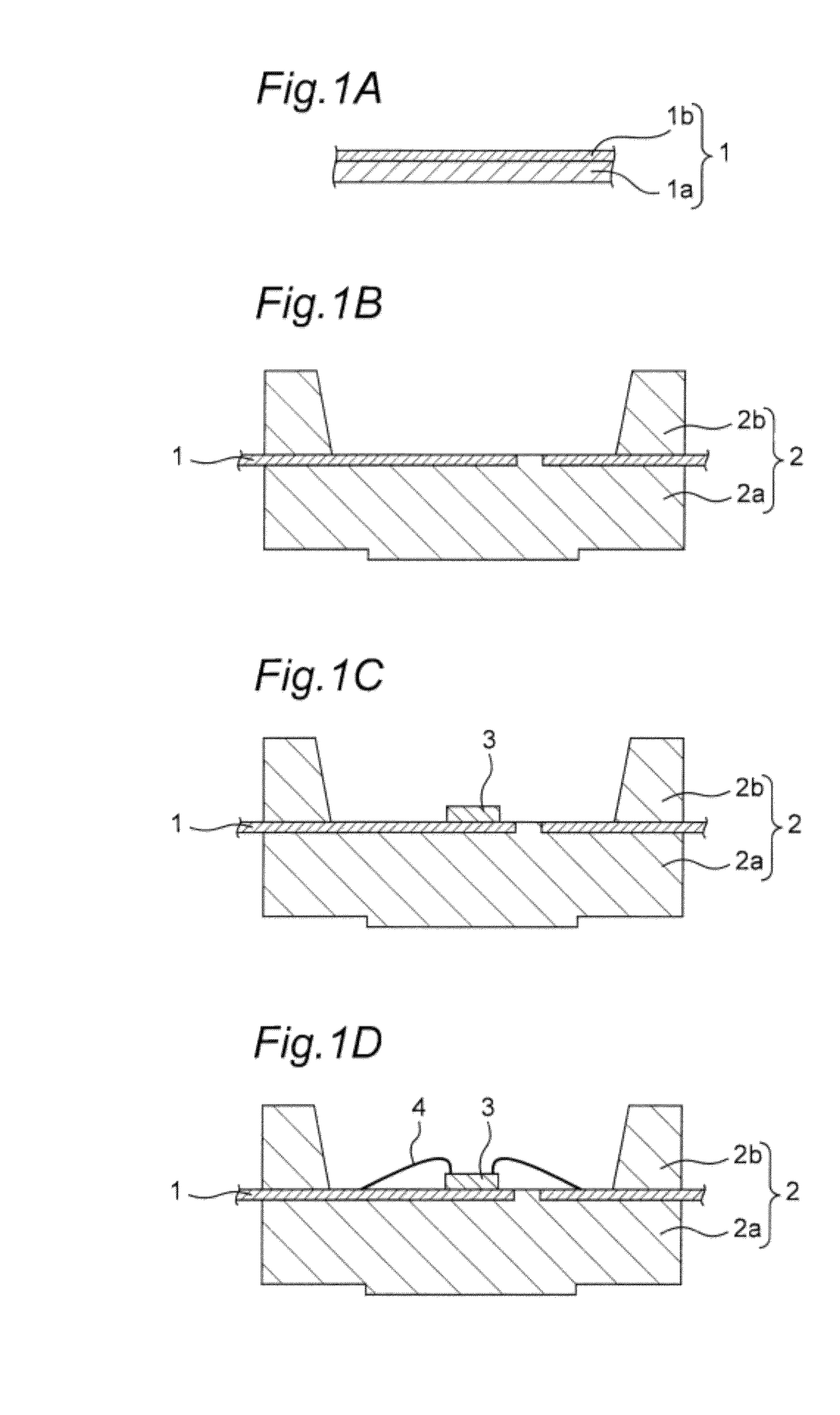
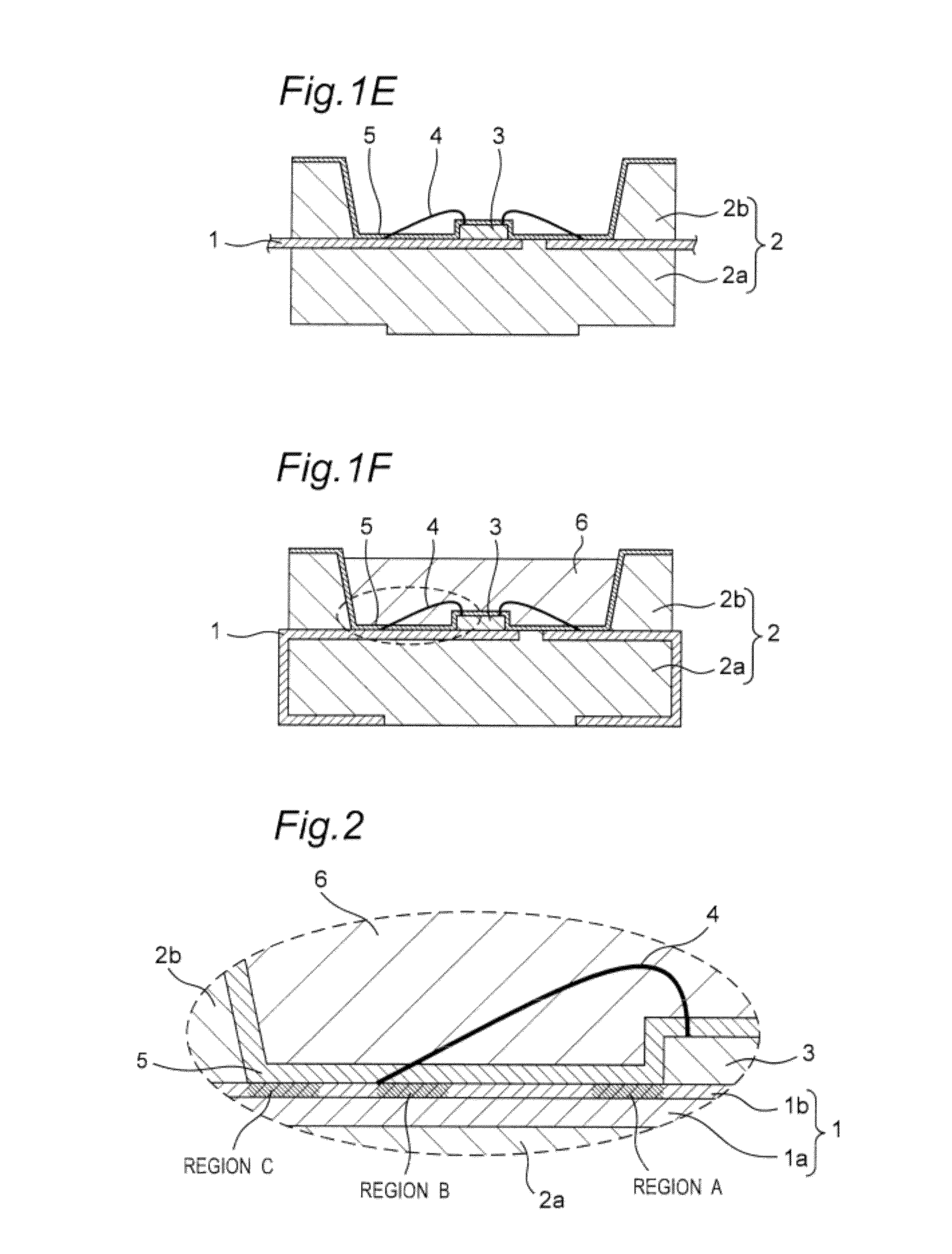
[0020]FIGS. 1A through 1F show each step of a method of manufacturing a light emitting device according to the present embodiment.

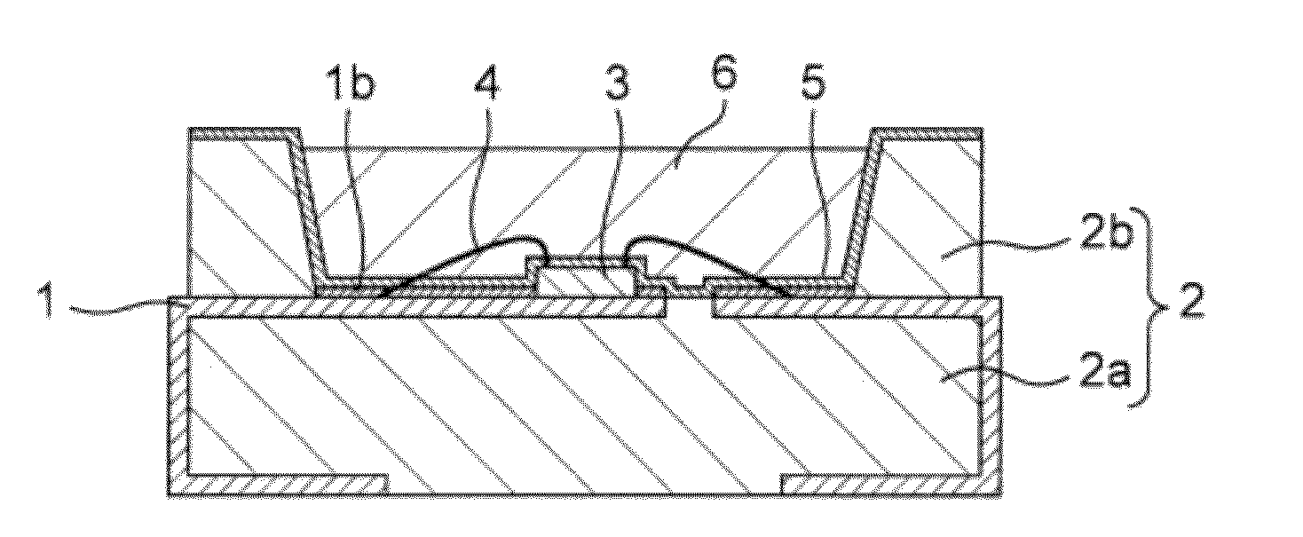
[0021]FIG. 2 is a magnified schematic view of the portion encircled with dashed line in FIG. 1F.

(Electrically Conductive Member Preparation Step)

[0022]First, as shown in FIG. 1A, an electrically conductive member 1 having a reflective film 1b provided on a base member 1a is prepared (electrically conductive member preparation step). In this embodiment, not only the base member 1a but also the reflective film 1b also has an electric conductivity. In the present embodiment, the electrically conductive member is constituted with a base member and a reflective film.

[0023]The material of the base member 1a is not specifically limited as long as it has electric conductivity. For the base member 1a, for example, copper or a copper alloy can be used.

[0024]The material of the reflective film 1b is not specifically limited as long as it is capable of reflecting lig...

second embodiment

[0057]The present embodiment will be described below with reference to FIGS. 3A to 3G. In this embodiment, like members as in the first embodiment are designated by like numerals and their repeated description will be omitted.

(Electrically Conductive Member Preparation Step)

[0058]First, as shown in FIG. 3A, the electrically conductive member 1 is prepared (electrically conductive member preparation step). In the present embodiment, different from that in the first embodiment, the electrically conductive member is made of the base member alone, and the reflective film 1b is not provided in this step.

(Package Forming Step)

[0059]Next, as shown in FIG. 3B, a package 2 having a base portion 2a and a side wall 2b provided on an electrically conductive member 1 can be formed (Package Forming Step).

(Light Emitting Element Disposing Step)

[0060]Next, as shown in FIG. 3C, a light emitting element 3 is disposed on the electrically conductive member 1 (light emitting element disposing step). Mor...


PUM


Abstract

Provided is a method of manufacturing a light emitting device capable of maintaining high optical output power while suppressing discoloration of the reflective film. A method of manufacturing a light emitting device according to an embodiment includes steps in an order of, preparing an electrically conductive member provided with a reflective film, disposing a light emitting element on the reflective film, and forming a protective film on the reflective film by using an atomic layer deposition method.

Description

BACKGROUND OF THE INVENTION[0001]1. Field of the Invention[0002]The present invention relates to a method of manufacturing a light emitting device having a light emitting element disposed on an electrically conductive member.[0003]2. Description of Related Art[0004]Attempts have been made in a light emitting device using a light emitting element as a light source to improve optical output power by disposing a reflective film containing silver and the like around the light emitting element, and further to suppress discoloration or the like of a reflective film by forming a protective film made of an inorganic material by way of sputtering, CVD or the like (see for example, Patent reference 1: JP 2009-224538A).[0005]Patent reference 1: JP 2009-224538A[0006]However, when a conventional method is used, there has been a problem that although the optical output power can be improved by the reflective film, decrease in optical output power occurs during the operation. That is, in the case ...

Claims


Application Information

Patent Timeline
Patent Type & Authority Applications(United States)
IPC IPC(8): H01L33/60H01L33/48
CPCH01L33/44H01L33/62H01L2224/48091H01L2224/48247H01L33/60H01L2924/09701H01L33/502H01L2924/00014H01L33/48H01L2924/181H01L2224/48257H01L2224/8592H01L2924/00012H01L33/32H01L33/483H01L33/38
Inventor WAKAKI, TAKAYOSHI
Owner NICHIA CORP
Why Eureka
Try Eureka