

Laser COD eliminating method suitable for mass production
A laser and mass-volume technology, applied in the direction of lasers, laser components, semiconductor lasers, etc., can solve problems such as defects at the acceleration interface, unsuitable for industrialized mass production, and inability to significantly increase the COD optical power threshold, so as to improve the bearing capacity , Improve the effect of light output power
- Summary
- Abstract
- Description
- Claims
- Application Information
AI Technical Summary
Problems solved by technology
Method used
Image

Examples
specific Embodiment
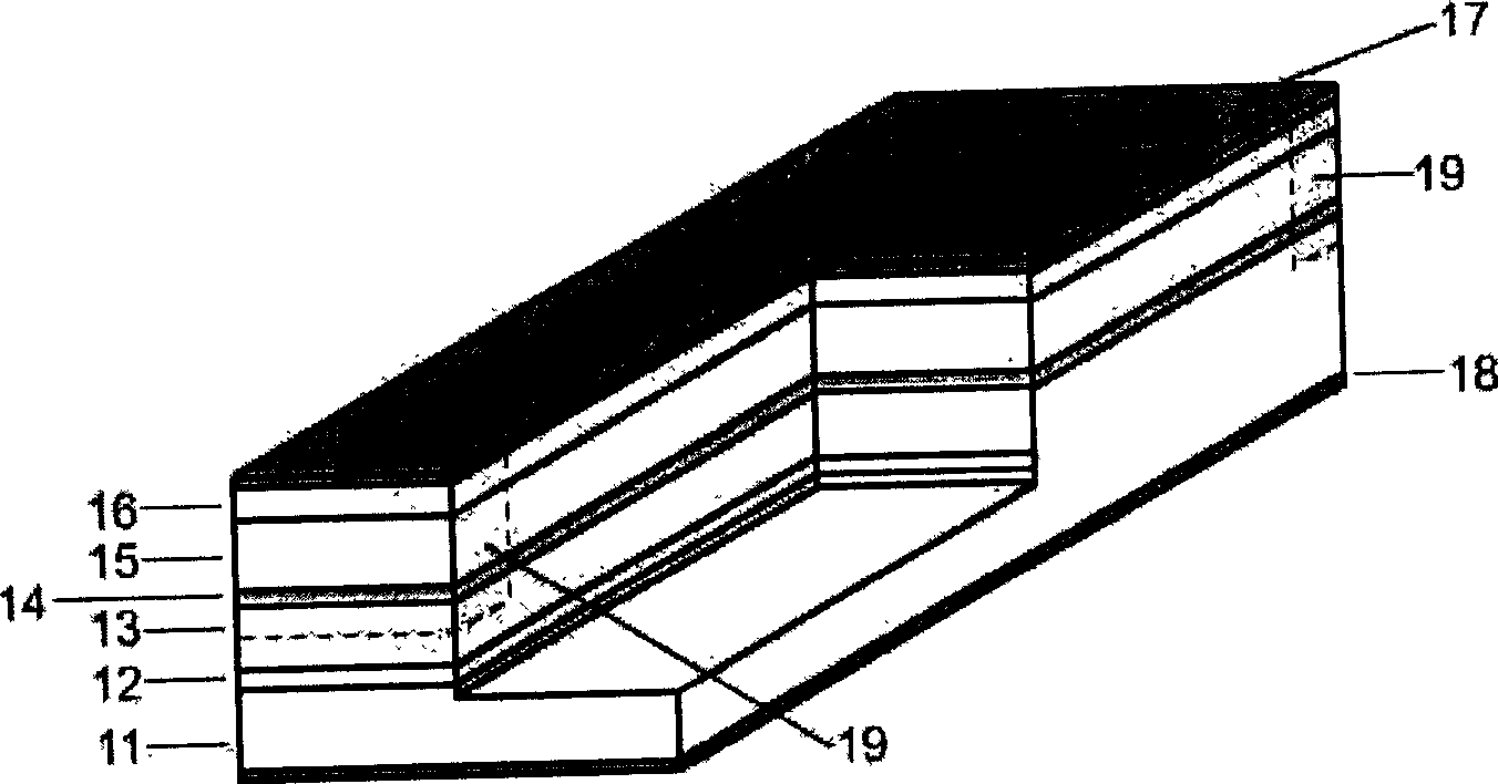
[0026] A specific technical process of a laser COD elimination method suitable for mass production according to a specific embodiment of the present invention will be described in detail below in conjunction with the accompanying drawings.
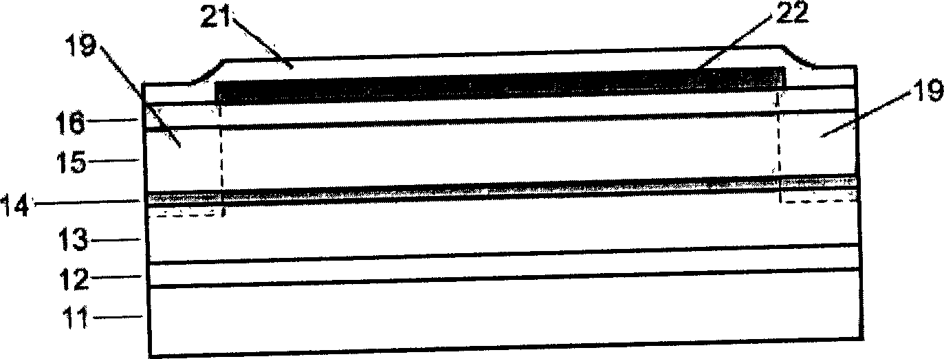
[0027] The present invention selectively mixes quantum wells on epitaxial wafers of semiconductor materials for making lasers. The actual operation is simple, and the process steps are as follows. Please refer to figure 2 :
[0028] (1), production of solid zinc source
[0029] First grow a dense silicon oxynitride layer 22 on the epitaxial wafer of semiconductor material for making the laser, and etch the silicon oxynitride layer on the end face of the laser. The etching solution is a hydrofluoric acid buffer solution. This etching solution is harmful to the laser. The surface has little effect. Then, a zinc oxide layer 21 is grown on the silicon oxynitride layer 22 and the electrode contact layer 16 of the semiconductor laser at a gro...
PUM
 Abstract
Description
Claims
Application Information