Preparation method of low noise GaN HEMT device

A low-noise, device technology, applied in the field of preparation of low-noise GaN HEMT devices, to prevent the deterioration of frequency characteristics, facilitate process integration, and reduce effects

Active Publication Date: 2014-05-07
NO 55 INST CHINA ELECTRONIC SCI & TECHNOLOGYGROUP CO LTD
View PDF7 Cites 19 Cited by
  • Summary
  • Abstract
  • Description
  • Claims
  • Application Information

AI Technical Summary

Problems solved by technology

[0004] The present invention proposes a preparation method of a low-noise GaN HEMT device, the purpose of which is to address these problems encountered by the low-noise GaN HEMT device, and to improve the noise performance of the device by using a composition-graded AlGaN back barrier structure

Method used


Image

  • Preparation method of low noise GaN HEMT device
  • Preparation method of low noise GaN HEMT device
  • Preparation method of low noise GaN HEMT device

Examples


preparation example Construction

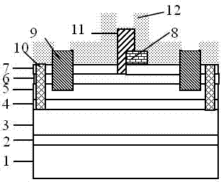
[0028] control Figure 2-1-Figure 2-6, a fabrication method of a low-noise GaN HEMT device, comprising:

[0029] Step 1) Use MOCVD equipment to grow AlGaN / GaN heterojunction materials with composition graded back barriers on semi-insulating SiC or sapphire substrates, such as diagram 2-1 shown;

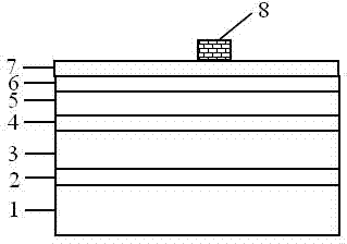
[0030] Step 2) On the clean AlGaN / GaN heterojunction material with compositional graded back barrier, define a dielectric field plate pattern on the sample by throwing the positive resist, exposing, and developing, and deposit multiple layers on the sample by low-temperature dielectric deposition method A layer of high dielectric constant dielectric material is used to form a dielectric field plate through the method of positive resist peeling, such as Figure 2-2 shown;

[0031] Step 3) On the sample obtained in step 2), define the source and drain regions on the sample by throwing the positive glue, exposing and developing, and use the plasma etching method to remove the source ...

Embodiment

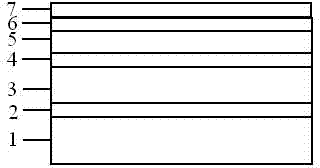
[0037] 1) On the semi-insulating 4H-SiC substrate 1, use MOCVD equipment to epitaxy the AlGaN / GaN heterojunction material with a composition gradient back barrier, first grow a 50nm low-temperature AlN nucleation layer 2, and then grow a 1 micron AlGaN composition Graded layer 3, composition graded AlGaN back barrier layer from AlN interface to GaN interface, Al composition is linearly graded from 0.5 to 0.04, and then grows 200nm GaN channel layer 4; 20nm Al 0.25 Ga 0.75 N barrier layer 5, Si doping concentration 1E18 cm thick 2nm -3 doped GaN capping layer 6 and a thickness of 2nm Si 3 N 4 protective layer 7;

[0038] 2) Clean the surface of the grown AlGaN / GaN heterojunction sample first, ultrasonically clean it in acetone and ethanol solutions for 5 minutes, rinse it in deionized water, and blow it dry with nitrogen;

[0039] 3) Coat AZ7908 positive-type photoresist on the sample by spin coating method, the uniform rotation speed is 5000rpm, and the uniform time is 20 ...


PUM


Abstract

The invention provides a preparation method of a low noise GaN HEMT device. The preparation method comprises the steps that 1) an AlGaN / GaN heterojunction material with a component gradient back barrier grows; 2) a medium field plate is prepared; 3) ohmic contact is prepared; 4) an isolation region of the device is formed; 5) a gamma type gate of a TaN radical is formed through a positive photoresist stripping method; 6) by using a plasma deposition method, a Si3N4 / SiO2 / Si3N4 multilayer surface passivation medium is deposited on the surface of a sample; and 7) through a plasma etching method, dielectric materials on a source drain and a gate electrode are removed, so as to form a test window. The preparation method has the advantages that 1) a structure is compatible with power GaN HEMT, which is conductive to process integration; 2) voltage resistance of the device is effectively improved, and the degradation of frequency characteristics is prevented; 3) the device's ability to bear high input power is improved; and 4) the effect of a passivation process on the device frequency is reduced, and at the same time the gate stability is improved.

Description

technical field [0001] The present invention relates to a preparation method of a low-noise GaN HEMT device, which uses a composition-graded AlGaN back barrier structure that can significantly improve the confinement of two-dimensional electron gas in the channel to improve the noise performance of the GaN HEMT device. The manufacture of the plate and the highly stable TaN gate improves the withstand voltage characteristics and temperature stability of the device, thereby improving the ability of the device to withstand high input power on the basis of improving the noise performance of the low-noise GaN HEMT device, and belongs to the technical field of semiconductor device preparation. technical background [0002] GaN-based wide bandgap semiconductor materials have the advantages of wide bandgap, high critical breakdown field strength, high temperature resistance and good chemical corrosion resistance. GaN HEMT devices made of AlGaN / GaN heterojunction have similar noise ch...

Claims


Application Information

Patent Timeline
Patent Type & Authority Applications(China)
IPC IPC(8): H01L21/335H01L21/28
CPCH01L29/405H01L29/66462
Inventor 周建军孔岑陈堂胜
Owner NO 55 INST CHINA ELECTRONIC SCI & TECHNOLOGYGROUP CO LTD
Why Eureka
Try Eureka