Semiconductor device

a semiconductor and semiconductor technology, applied in the direction of semiconductor devices, basic electric elements, electrical appliances, etc., can solve the problems of difficult selective separation of micro-sized light-emitting diodes from wafers, easy to be confused, and susceptible to external impacts, so as to prevent the breakage of an insulating layer, improve optical output power, and easy to understand

Active Publication Date: 2021-02-04
LG INNOTEK CO LTD
View PDF0 Cites 11 Cited by
  • Summary
  • Abstract
  • Description
  • Claims
  • Application Information

AI Technical Summary

Benefits of technology

[0016]According to an embodiment, it is possible to make a semiconductor device robust to external impacts. Accordingly, it is possible to solve a problem of a semiconductor being damaged during a transfer process.
[0017]Also, it is possible to manufacture a semiconductor element with improved optical output power.
[0018]Also, it is possible to prevent an insulating layer from being broken when a semiconductor device is being separated from a wafer.

Problems solved by technology

However, micro-sized light-emitting diodes have a problem of being susceptible to external impacts.
Also, micro-sized light-emitting diodes have another problem of being difficult to selectively separate from a wafer.
In particular, defects occur when the light-emitting diodes are transferred to another substrate due to particles remaining when separation occurs.

Method used


Image

  • Semiconductor device
  • Semiconductor device
  • Semiconductor device

Examples


Embodiment Construction

[0035]The following embodiments may be modified or combined with each other, and the scope of the present invention is not limited to the embodiments.

[0036]Details described in a specific embodiment may be understood as descriptions associated with other embodiments unless otherwise stated or contradicted even if there is no description thereof in the other embodiments.

[0037]For example, when features of element A are described in a specific embodiment and features of element B are described in another embodiment, an embodiment in which element A and element B are combined with each other should be understood as falling within the scope of the present invention unless otherwise stated or contradicted even if not explicitly stated.

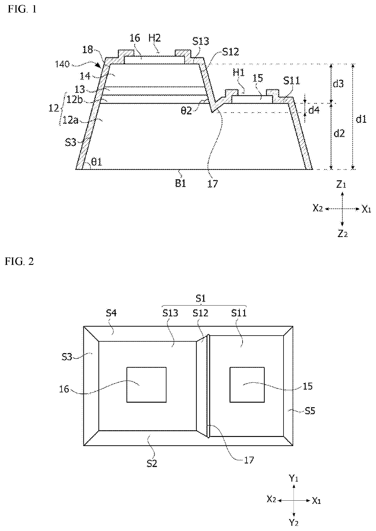
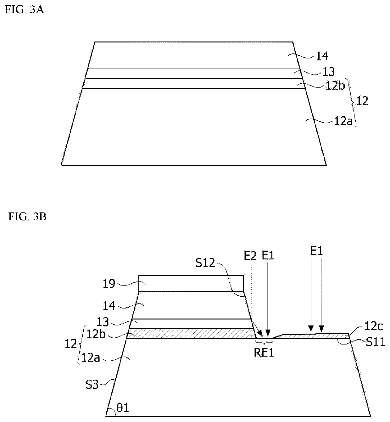
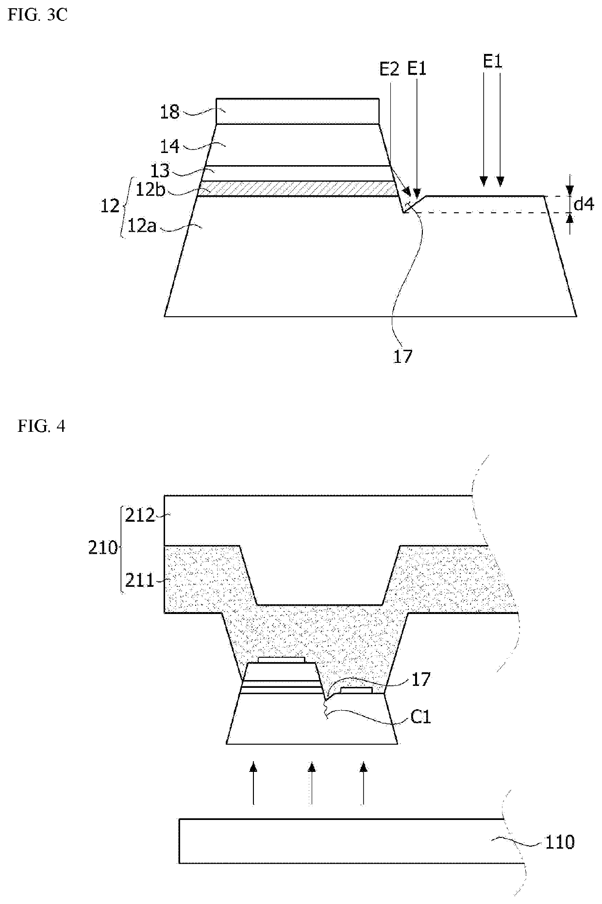
[0038]In the descriptions of embodiments, when an element is referred to as being above or under another element, the two elements may be in direct contact with each other, or one or more other elements may be disposed between the two elements. In addition,...


PUM

PropertyMeasurementUnit
vertical heightaaaaaaaaaa
angleaaaaaaaaaa
angleaaaaaaaaaa

Abstract

Disclosed is a semiconductor device including a semiconductor structure including a first semiconductor layer, a second semiconductor layer, and an active layer disposed between the first semiconductor layer and the second semiconductor layer, a first electrode electrically connected to the first semiconductor layer, and a second electrode electrically connected to the second semiconductor layer. The semiconductor structure includes a first upper surface on which the first semiconductor layer is exposed, a second upper surface on which the second semiconductor layer is disposed, an inclined surface connecting the first upper surface and the second upper surface, and a recess formed between the first upper surface and the inclined surface. The recess has a depth less than or equal to 30% of a vertical distance between the first upper surface and the second upper surface.

Description

TECHNICAL FIELD[0001]Embodiments relate to a semiconductor device, a semiconductor device array, and a manufacturing method thereof.BACKGROUND ART[0002]A light-emitting diode (LED) is a light-emitting device that emits light when an electric current is applied thereto. A light-emitting diode can emit light with high efficiency at a low voltage, thus significantly saving energy. Recently, the luminance problem of light-emitting diodes has been greatly mitigated, and thus light-emitting diodes are being applied to various types of apparatuses such as backlight units of liquid crystal displays, display boards, display apparatuses, and home appliances.[0003]Semiconductor devices including compounds such as GaN and AlGaN have many merits such as wide and adjustable band gap energy and thus may be variously used as light-emitting elements, light-receiving elements, various kinds of diodes, or the like.[0004]In particular, light-emitting elements such as a light-emitting diode or a laser d...

Claims


Application Information

Patent Timeline
Patent Type & Authority Applications(United States)
IPC IPC(8): H01L33/20H01L25/075H01L33/00H01L25/16
CPCH01L33/20H01L25/0753H01L25/167H01L33/0066H01L33/0093H01L33/30H01L27/156H01L33/0095
Inventor LEE, SANG YOULKIM, CHUNG SONGMOON, JI HYUNGPARK, SUN WOOCHO, HYEON MIN
Owner LG INNOTEK CO LTD
Why Eureka
Try Eureka