High-power semiconductor laser device in which near-edge portions of active layer are removed

Inactive Publication Date: 2001-08-30
FUJIFILM HLDG CORP
View PDF0 Cites 13 Cited by
  • Summary
  • Abstract
  • Description
  • Claims
  • Application Information

AI Technical Summary

Problems solved by technology

However, when the optical power is maximized, currents generated by optical absorption in the vicinity of end faces generate heat, i.e., raise the temperature at the end faces.
This damage is the so-called catastrophic optical mirror damage (COMD).
When the optical power reaches the COMD level, the optical output deteriorates with time.
Further, the semiconductor laser device is likely to suddenly break down due to the COMD.
Therefore, the above semiconductor l

Method used


Image

  • High-power semiconductor laser device in which near-edge portions of active layer are removed
  • High-power semiconductor laser device in which near-edge portions of active layer are removed
  • High-power semiconductor laser device in which near-edge portions of active layer are removed

Examples


Example

First Embodiment

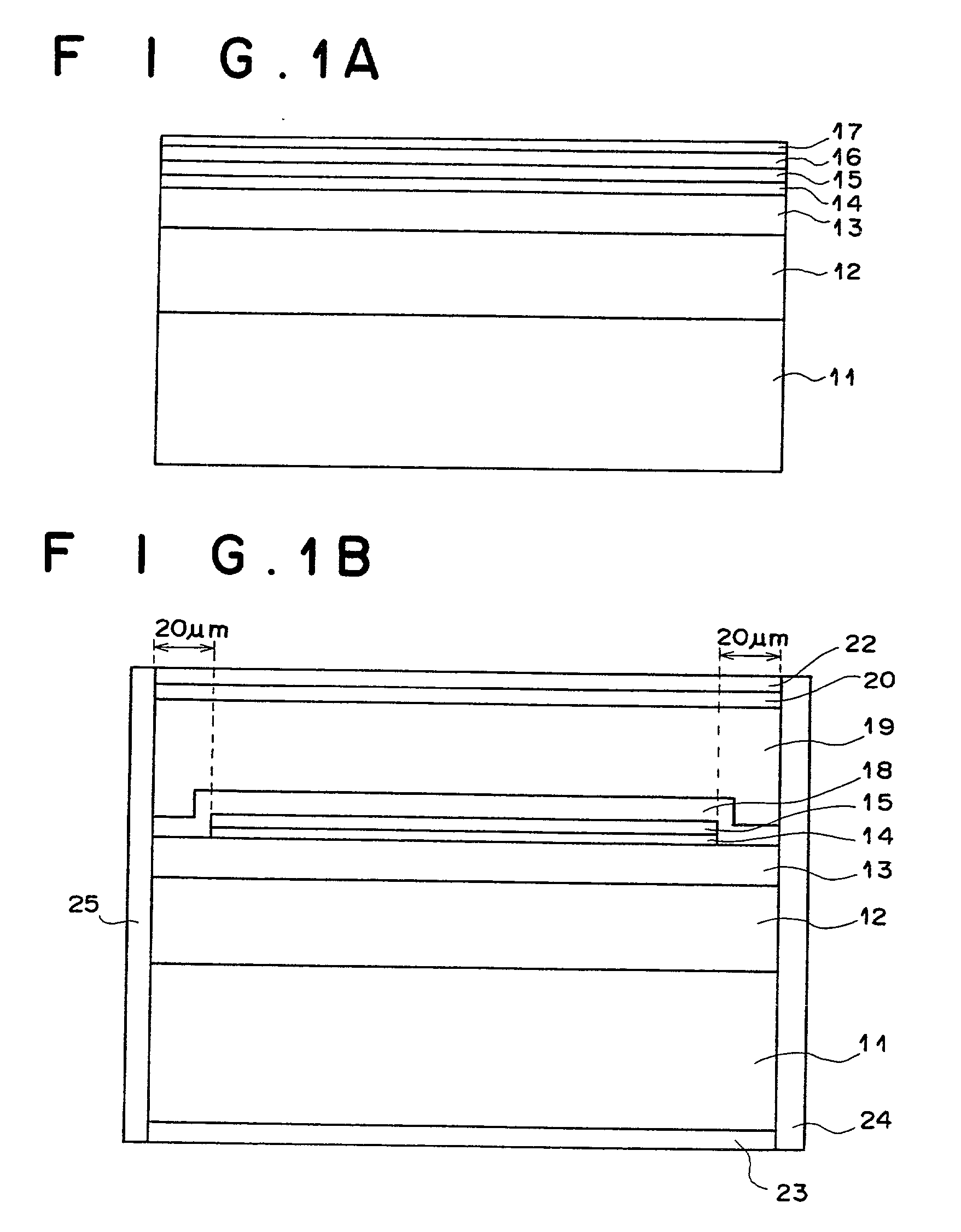
[0028] FIG. 1A is a cross-sectional view of a representative intermediate stage in a process for producing a semiconductor laser device as the first embodiment of the present invention, and FIG. 1B is a cross-sectional view of the semiconductor laser device as the first embodiment of the present invention. The cross sections exhibited in FIGS. 1A and 1B are parallel to the direction of the laser light emitted from the semiconductor laser device.

[0029] First, as illustrated in FIG. 1A, an n-type Al.sub.z1Ga.sub.1-z1As lower cladding layer 12 (0.55.ltoreq.z1.ltoreq.0.8), an n-type or i-type In.sub.0.49Ga.sub.0.51P lower optical waveguide layer 13, an In.sub.x1Ga.sub.1-x3As.sub.1-y3P.sub.y3 quantum well active layer 14 (0.ltoreq.x3.ltoreq.0.4, 0.ltoreq.y3.ltoreq.0.5), a p-type or i-type In.sub.0.49Ga.sub.0.51P first upper optical waveguide layer 15, and a GaAs cap layer 16 having a thickness of approximately 10 nm are formed on an n-type GaAs substrate 11 by organometal...

Example

Second Embodiment

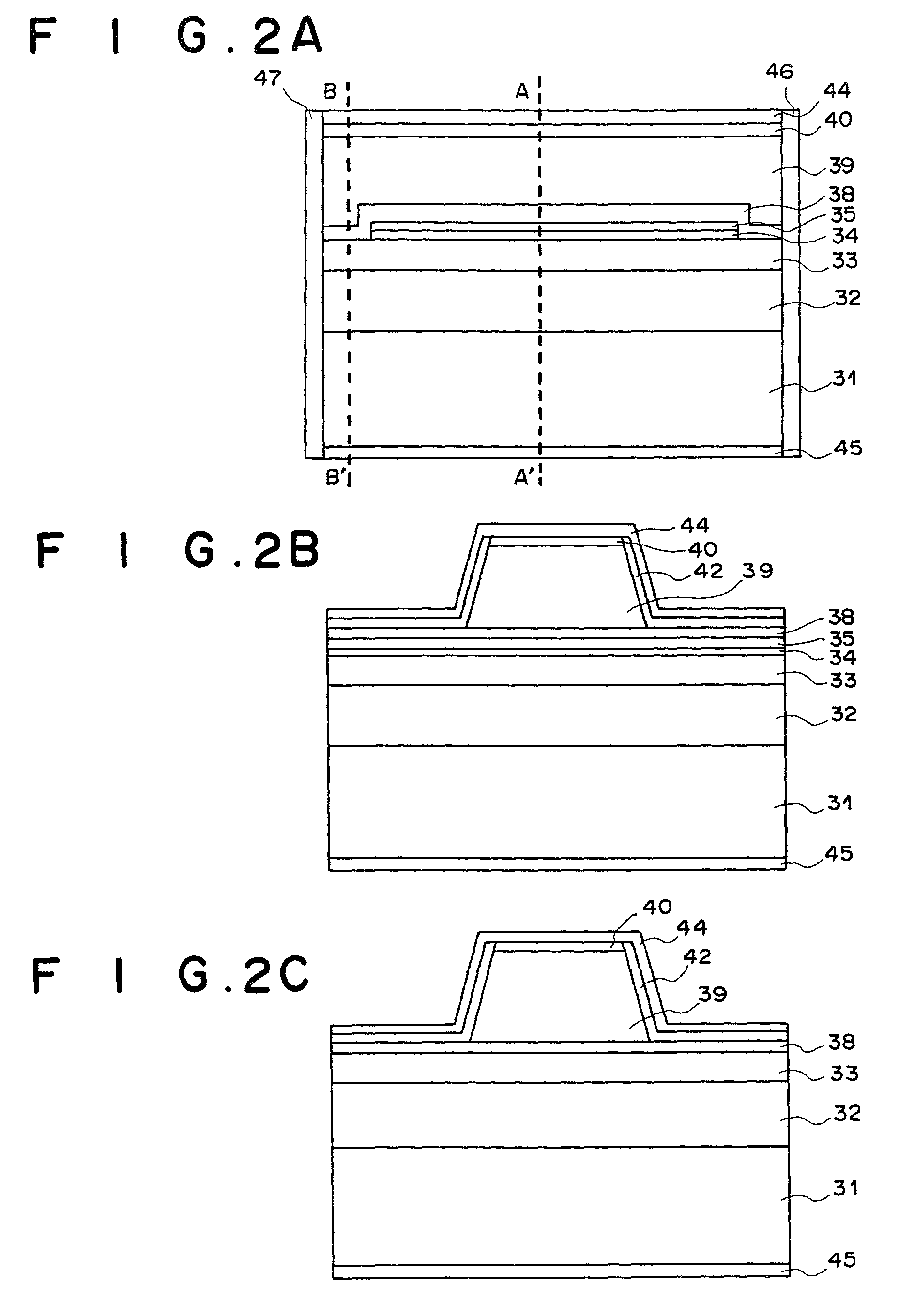
[0038] FIGS. 2A to 2C are cross-sectional views of a semiconductor laser device as the second embodiment of the present invention. The cross section shown in FIG. 2A is parallel to the direction of the laser light emitted from the semiconductor laser device. FIG. 2B shows the cross section B-B' in the vicinity of the end face, and FIG. 2C shows the cross section A-A' in the central portion of the semiconductor laser device.

[0039] First, as illustrated in FIG. 2A, an n-type Al.sub.z1Ga.sub.1-z1As lower cladding layer 32 (0.55.ltoreq.zl.ltoreq.0.8), an n-type or i-type In.sub.0.49Ga.sub.0.51P lower optical waveguide layer 33, an In.sub.x3Ga.sub.1-x3As.sub.1-y3P.sub.y3 quantum well active layer 34 (0.ltoreq.x3.ltoreq.0.3, 0.ltoreq.y3.ltoreq.0.5), a p-type or i-type In.sub.0.49Ga.sub.0.51P first upper optical waveguide layer 35, and a GaAs cap layer 36 (not shown) having a thickness of approximately 10 nm are formed on an n-type GaAs substrate 31 by organometallic vapor...

Example

Third Embodiment

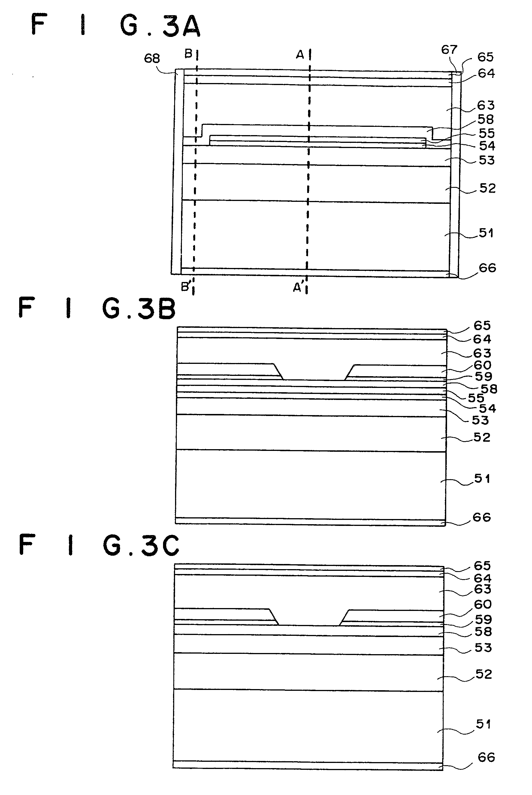
[0048] FIGS. 3A to 3C are cross-sectional views of a semiconductor laser device as the third embodiment of the present invention. The cross section shown in FIG. 3A is parallel to the direction of the laser light emitted from the semiconductor laser device. FIG. 3B shows the cross section B-B' in the vicinity of the end face, and FIG. 3C shows the cross section A-A' in the central portion of the semiconductor laser device.

[0049] First, as illustrated in FIG. 3A, an n-type In.sub.0.49(Ga.sub.1-z2-Al.sub.z2).sub.0.51P lower cladding layer 52 (0.1.ltoreq.z2


PUM


Abstract

In a semiconductor laser device, a GaAs substrate of a first conductive type, a lower cladding layer of the first conductive type, a lower optical waveguide layer made of InGaP of an undoped type or the first conductive type, an active layer made of InGaAsP or InGaAs, a first upper optical waveguide layer made of InGaP of an undoped type or a second conductive type, a second upper optical waveguide layer made of InGaP of an undoped type or the second conductive type, an upper cladding layer of the second conductive type, and a contact layer of the second conductive type are formed in this order to form a layered structure. Near-edge portions of the active layer and the first upper optical waveguide layer, which are adjacent to opposite end faces of the layered structure, are removed, and the second upper optical waveguide layer is formed over the first upper optical waveguide layer and near-edge areas of the lower optical waveguide layer, where the opposite end faces are perpendicular to the direction of laser light which oscillates in the semiconductor laser device.

Description

[0001] 1. Field of the Invention[0002] The present invention relates to a semiconductor laser device which emits laser light having a wavelength of 0.7 to 1.2 .mu.m.[0003] 2. Description of the Related Art[0004] In many conventional semiconductor laser devices which emit laser light having a wavelength of 0.7 to 1.2 .mu.m, a current confinement structure and an index-guided structure are provided in crystal layers constituting each semiconductor laser device so that each semiconductor laser device oscillates in a fundamental transverse mode.[0005] For example, J. K. Wade et al. ("6.1 W continuous wave front-facet power from Al-free active-region (.lambda.=805 nm) diode lasers," Applied Physics Letters, vol. 72, No. 1, 1998, pp.4-6) disclose a semiconductor laser device which emits light in the 805 nm band. The semiconductor laser device comprises an Al-free InGaAsP active layer, an InGaP optical waveguide layer, and InAlGaP cladding layers. In addition, in order to improve the chara...

Claims


Application Information

Patent Timeline
IPC IPC(8): H01S5/16H01S5/20H01S5/22H01S5/223H01S5/343
CPCB82Y20/00H01S5/164H01S5/168H01S5/2004H01S5/2231H01S5/34313H01S5/3436H01S5/34386
Inventor FUKUNAGA, TOSHIAKI
Owner FUJIFILM HLDG CORP
Why Eureka
Try Eureka