Charge sharing system and method of lcos display

Inactive Publication Date: 2012-03-01
SHENZHEN YANGTZE LIVETECH
2 Cites 0 Cited by

AI-Extracted Technical Summary

Problems solved by technology

However, in most cases, the LCD displays color images, that is, adjacent sub-pixel points display different data, which leads to varied voltage amplitudes between adjacent pixels R1 and G1, B1 and R2, and G2 and B2, so that the voltage fails to be sufficiently neutralized, and the reduced...

Method used

[0040]Through the above charge system, the voltage of all the sub-pixels in the pixel matrix 3 is changed into VH/4+3VL/4 or VL/4+3VH/4, that is, the dynamic power consumption is reduced by 75%. Meanwhile, the control circuit 4 controls the turn-off and the turn-on of the buffer 12 and the gamma reference voltage circuit 6, so that the static power consumption of the column driving circuit 1 and the display system is reduced, the charge use efficiency of the display is improved, and the power consumption of the LCoS display system is lowered.
[0043]In view of the above, through the improved charge sharing system of an LCoS display provided in the embodiment of the present invention, the dynamic power consumption is reduced by 75%. Meanwhile, the control circuit controls the turn-off and the turn-on of the buffer and the gamma reference voltage circuit, so that the static power consumption of the column driving circuit and the display system is reduced, the charge use efficiency of the display is improved, and the power consumption of the LCoS display system is lowered.
[0053]It can be known from the...

Benefits of technology

[0008]In order to further reduce the dynamic power consumption of the LCoS driving circuit system, and lower the static power consumption of the co...

Abstract

In the field of a liquid crystal on silicon (LCoS) display, a charge sharing system and a charge sharing method of an LCoS display are provided. The system includes: a column driving circuit, a row driving circuit, a pixel matrix, a control circuit, a gamma reference voltage circuit, and a first switching module. The column driving circuit includes a second switching module, a buffer, a shift register, a latch, and a digital-to-analog (D/A) converter. The second switching module is serially connected between the D/A converter and the buffer. The control circuit simultaneously outputs a signal for controlling turn-off of the buffer, a signal for controlling turn-off of a switch in the second switching module, and a signal for controlling turn-off of the gamma reference voltage circuit. The control circuit outputs a signal for controlling turn-on of a switch in the first switching module. The control circuit outputs a signal for controlling the row driving circuit. The control circuit simultaneously outputs a signal for controlling turn-on of the buffer, a signal for controlling turn-on of the switch in the second switching module, and a signal for controlling turn-on of the gamma reference voltage circuit.

Application Domain

Technology Topic

Image

  • Charge sharing system and method of lcos display
  • Charge sharing system and method of lcos display
  • Charge sharing system and method of lcos display

Examples

  • Experimental program(2)

Example

Embodiment 1
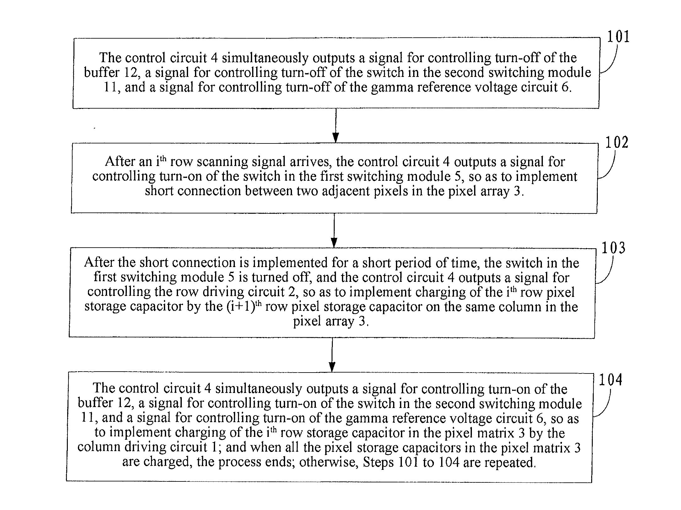
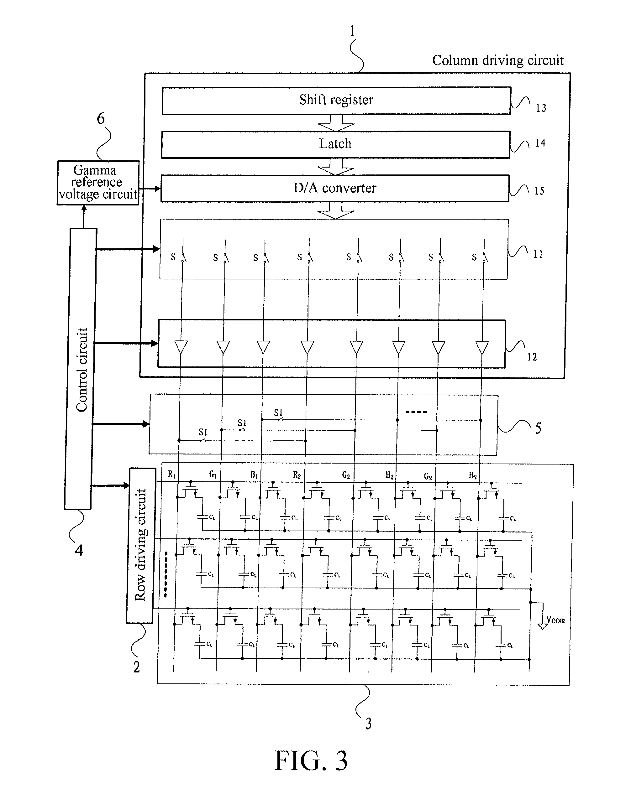
[0032]In order to further reduce the dynamic power consumption of the LCoS driving circuit system, and lower the static power consumption of the column driving circuit and the display system, the present invention provides a charge sharing system of an LCoS display, and the details are described in the following with reference to FIG. 3.
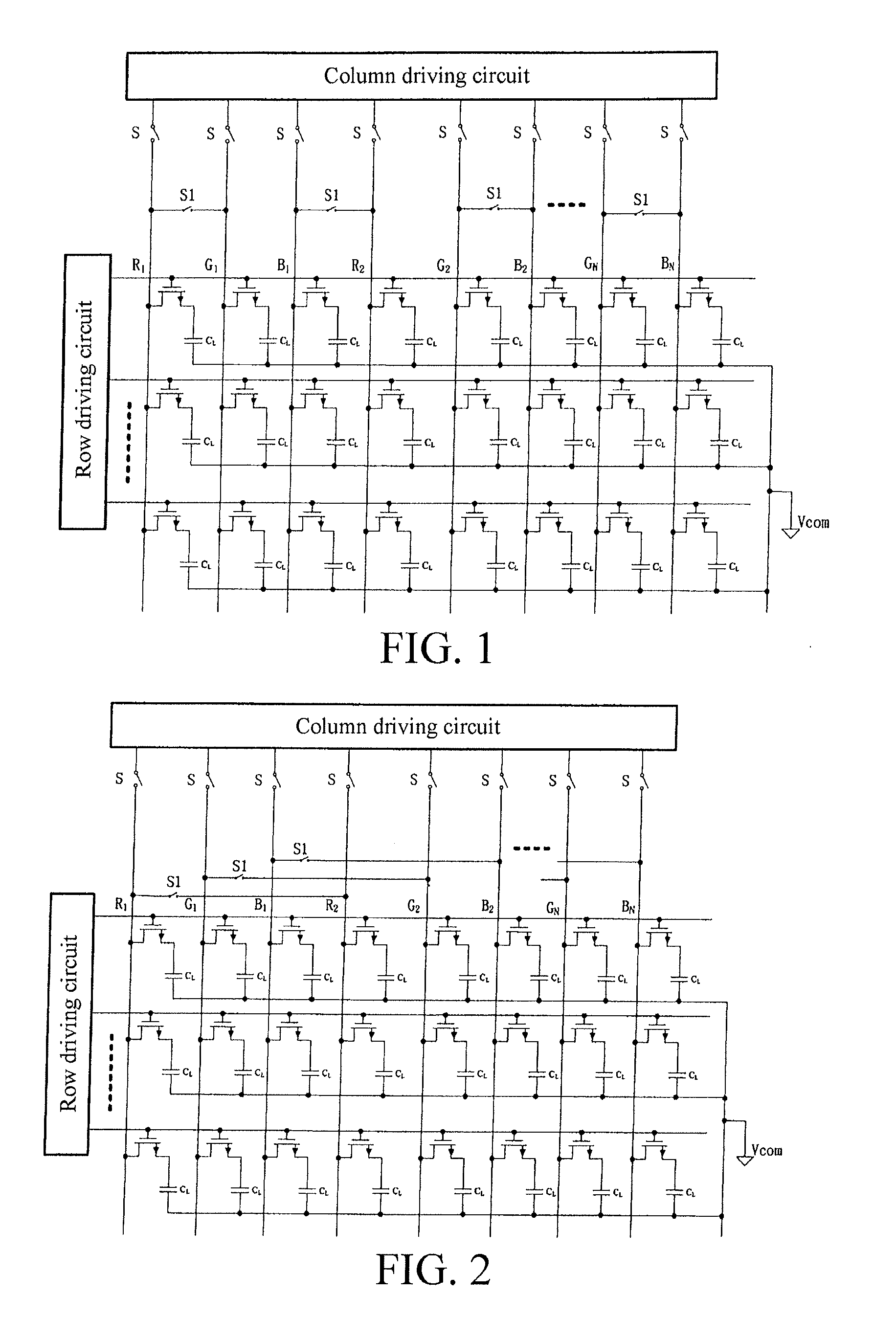
[0033]The spatial correlation of LCD display refers to that the colors of two adjacent pixels are identical or close. As the colors of most areas in an image change gradually, the colors of two adjacent pixels are close or identical in most cases. Therefore, sub-pixels having the same color attribute in the two adjacent pixels (each pixel consists of three consecutive sub-pixels) have the same voltage amplitude but opposite polarities. The temporal correlation of the LCD display refers to that displayed images of two consecutive frames are identical or close, so that the sub-pixels having the same color attribute in the two pixels have the same voltage amplitude but opposite polarities.
[0034]The charge sharing system of an LCoS display in the present invention includes: a column driving circuit 1, a row driving circuit 2, a pixel matrix 3, a control circuit 4, a first switching module 5, and a gamma reference voltage circuit 6. The column driving circuit 1 includes: a second switching module 11, a buffer 12, a shift register 13, a latch 14, and a D/A converter 15. The second switching module 11 is serially connected between the D/A converter 15 and the buffer 12.
[0035]The control circuit 4 is used for simultaneously outputting a signal for controlling turn-off of the buffer 12, a signal for controlling turn-off of a switch in the second switching module 11, and a signal for controlling turn-off of the gamma reference voltage circuit 6.
[0036]The control circuit 4 is used for outputting a signal for controlling turn-on of a switch in the first switching module 5, so as to implement short connection between two adjacent pixels in the pixel array 3. The control circuit 4 is used for outputting a signal for controlling the row driving circuit 2, so as to implement charging of an ith row pixel storage capacitor by an (i+1)th row pixel storage capacitor on the same column in the pixel array 3, where i=1, 2, . . . , M−1, and M is the number of rows of the pixels.
[0037]The control circuit 4 is used for simultaneously outputting a signal for controlling turn-on of the buffer 12, a signal for controlling turn-on of the switch in the second switching module 11, and a signal for controlling turn-on of the gamma reference voltage circuit 6, so as to implement charging of the storage capacitors in the pixel matrix 3 by the column driving circuit 1 when the buffer 12, the gamma reference voltage circuit 6, and the switch in the second switching module 11 are turned on.
[0038]Further, when the column driving circuit 1 does not charge the storage capacitors in the pixel matrix 3, the control circuit 4 sends a signal for controlling turn-off of the buffer 12 and the gamma reference voltage circuit 6.
[0039]Furthermore, the charge system is not only applicable to an LCoS color display system and an LCoS monochrome display system, but also applicable to a thin film transistor-liquid crystal display (TFT-LCD) color display system and a TFT-LCD monochrome display system.
[0040]Through the above charge system, the voltage of all the sub-pixels in the pixel matrix 3 is changed into VH/4+3VL/4 or VL/4+3VH/4, that is, the dynamic power consumption is reduced by 75%. Meanwhile, the control circuit 4 controls the turn-off and the turn-on of the buffer 12 and the gamma reference voltage circuit 6, so that the static power consumption of the column driving circuit 1 and the display system is reduced, the charge use efficiency of the display is improved, and the power consumption of the LCoS display system is lowered.
[0041]The specific operating process is described below with reference to FIG. 3.
[0042]The control circuit 4 simultaneously outputs a signal for controlling turn-off of the buffer 12, a signal for controlling turn-off of the switch in the second switching module 11, and a signal for controlling turn-off of the gamma reference voltage circuit 6. After an ith row scanning signal arrives, the control circuit 4 outputs a signal for controlling turn-on of the switch in the first switching module 5, so as to implement short connection between two adjacent pixels in the pixel array 3, and the short connection may last for a short period of time. After the short connection is implemented, the switch in the first switching module 5 is turned off. The control circuit 4 outputs a signal for controlling the row driving circuit 2, so as to implement charging of the ith row pixel storage capacitor by the (i+1)th row pixel storage capacitor on the same column in the pixel array 3. The control circuit 4 simultaneously outputs a signal for controlling turn-on of the buffer 12, a signal for controlling turn-on of the switch in the second switching module 11, and a signal for controlling turn-on of the gamma reference voltage circuit 6, so as to implement charging of the ith row storage capacitor in the pixel matrix 3 by the column driving circuit 1 when the buffer 12, the gamma reference voltage circuit 6, and the switch in the second switching module 11 are turned on. Specifically, the switch in the first switching module 5 is turned on, and the storage capacitors of two adjacent pixels (Rk, Gk, Bk) and (Rk+1, Gk+1, Bk+1) are short-connected, that is, the storage capacitors of the three sub-pixels Rk and Rk+1, Gk and Gk+1 and Bk and Bk+1 are respectively short-connected, where k=1, 2, . . . , N−1, and N is the number of the sub-pixels. The control circuit 4 outputs a signal for controlling the row driving circuit 2, and loads a short-time scanning pulse to the (i+1)th row pixels next to the ith row, so as to implement short connection between the pixel storage capacitors on the same column of the ith row and the (i+1)th row, and to implement charging of the ith row pixel storage capacitor by the (i+1)th row pixel storage capacitor on the same column, where i=1, 2, . . . , M−1, and M is the number of rows of the pixels. Likewise, each row is charged by the next row, and the process is implemented till the last row is charged.
[0043]In view of the above, through the improved charge sharing system of an LCoS display provided in the embodiment of the present invention, the dynamic power consumption is reduced by 75%. Meanwhile, the control circuit controls the turn-off and the turn-on of the buffer and the gamma reference voltage circuit, so that the static power consumption of the column driving circuit and the display system is reduced, the charge use efficiency of the display is improved, and the power consumption of the LCoS display system is lowered.

Example

Embodiment 2
[0044]In order to further reduce the dynamic power consumption of the LCoS driving circuit system, and lower the static power consumption of the column driving circuit and the display system, the present invention provides a charge sharing method of an LCoS display, and the details are described in the following with reference to FIG. 3 and FIG. 4.
[0045]101: The control circuit 4 simultaneously outputs a signal for controlling turn-off of the buffer 12, a signal for controlling turn-off of the switch in the second switching module 11, and a signal for controlling turn-off of the gamma reference voltage circuit 6.
[0046]Specifically, when the LCoS displays a dynamic image, after the previous driving process is completed, the control circuit 4 outputs a signal for controlling turn-off of the switch in the second switching module 11 of the column driving circuit 1, so that the column driving circuit 1 and the pixel matrix 3 are disconnected, and simultaneously outputs a signal for controlling turn-off of the buffer 12 and the gamma reference voltage circuit 6.
[0047]102: After an ith row scanning signal arrives, the control circuit 4 outputs a signal for controlling turn-on of the switch in the first switching module 5, so as to implement short connection between two adjacent pixels in the pixel array 3, where i=1, 2, . . . , M−1, and M is the number of rows of the pixels.
[0048]Specifically, the storage capacitors of two adjacent pixels (Rk, Gk, Bk) and (Rk+1, Gk+1, Bk+1) are short-connected, that is, the storage capacitors of the three sub-pixels Rk and Rk+1, Gk and Gk+1, and Bk and Bk+1 in the two pixels (Rk, Gk, Bk) and (Rk+1, Gk+1, Bk+1) are respectively short-connected, where k=1, 2, . . . , N−1, and N is the number of the sub-pixels.
[0049]103: After the short connection is implemented for a short period of time, the switch in the first switching module 5 is turned off, and the control circuit 4 outputs a signal for controlling the row driving circuit 2, so as to implement charging of the ith row pixel storage capacitor by the (i+1)th row pixel storage capacitor on the same column in the pixel array 3.
[0050]Specifically, the control circuit 4 outputs a signal for controlling the row driving circuit 2, and loads a short-time scanning pulse to the (i+1)th row pixels, so as to implement short connection between the pixel storage capacitors on the same column of the ith row and the (i+1)th row, so as to implement charging of the ith row pixel storage capacitor by the (i+1)th row pixel storage capacitor on the same column, where i=1, 2, . . . , M−1, and M is the number of rows of the pixels.
[0051]104: The control circuit 4 simultaneously outputs a signal for controlling turn-on of the buffer 12, a signal for controlling turn-on of the switch in the second switching module 11, and a signal for controlling turn-on of the gamma reference voltage circuit 6, so as to implement charging of the ith row storage capacitor in the pixel matrix 3 by the column driving circuit 1. When all the pixel storage capacitors in the pixel matrix 3 are charged, the process ends; otherwise, Steps 101 to 104 are repeated.
[0052]Specifically, the control circuit 4 simultaneously outputs a signal for controlling turn-on of the buffer 12, a signal for controlling turn-on of the switch in the second switching module 11, and a signal for controlling turn-on of the gamma reference voltage circuit 6, and the column driving circuit 1 and the pixel matrix 3 are connected, so as to implement charging of the ith row storage capacitor in the pixel matrix 3 by the column driving circuit 1, thereby completing scanning of the ith row. When all the pixel storage capacitors in the pixel matrix 3 are charged, the process ends; otherwise, Steps 101 to 104 are repeated. Likewise, each row is charged by the next row, and the process is implemented till the last row is charged.
[0053]It can be known from the calculation method in the prior art that, through the above method, the voltage of all the sub-pixels in the pixel matrix 3 is changed into VH/4+3VL/4 or VL/4+3VH/4, that is, the dynamic power consumption is reduced by 75%. Meanwhile, the control circuit 4 controls the turn-off and the turn-on of the buffer 12 and the gamma reference voltage circuit 6, so that the static power consumption of the column driving circuit 1 and the display system is reduced, the charge use efficiency of the display is improved, and the power consumption of the LCoS display system is lowered.
[0054]In the actual implementation, the method may also be applied to a TFT-LCD display system.
[0055]In view of the above, through the improved charge sharing method of an LCoS display provided in the embodiment of the present invention, the dynamic power consumption is reduced by 75%. Meanwhile, the control circuit controls the turn-off and the turn-on of the buffer and the gamma reference voltage circuit, so that the static power consumption of the column driving circuit and the display system is reduced, the charge use efficiency of the display is improved, and the power consumption of the LCoS display system is lowered.
[0056]Persons skilled in the art may understand that the accompanying drawings are merely schematic views for illustrating an exemplary embodiment, and the serial numbers of the embodiments of the present invention are for illustration only, instead of indicating the preference of the embodiments.
[0057]Although the invention being described as some preferred embodiments, the scope for which the protection is sought by the present invention is not limited thereby. Various modifications and variations without departing from the scope or spirit of the invention should be considered falling within the scope of the present invention.

PUM

no PUM

Description & Claims & Application Information

We can also present the details of the Description, Claims and Application information to help users get a comprehensive understanding of the technical details of the patent, such as background art, summary of invention, brief description of drawings, description of embodiments, and other original content. On the other hand, users can also determine the specific scope of protection of the technology through the list of claims; as well as understand the changes in the life cycle of the technology with the presentation of the patent timeline. Login to view more.

Similar technology patents

Subthreshold SRAM memory cell

ActiveCN104916309AReduce dynamic power consumptionSignificant dynamic power consumptionDigital storageVIT signalsSram cell
Owner:锐立平芯微电子(广州)有限责任公司

Dynamic comparator circuit with low power consumption

Owner:UNIV OF ELECTRONIC SCI & TECH OF CHINA +1

Frame synchronization system and method for shortening total time length of calibration and synchronization

ActiveCN114465688ASave time at workReduce dynamic power consumptionTime-division multiplexTime delaysDynamic power dissipation
Owner:国芯科技(广州)有限公司

Classification and recommendation of technical efficacy words

  • Reduce dynamic power consumption

Automatic extension of clock gating technique to fine-grained power gating

ActiveUS20070024318A1Reduce dynamic power consumptionPower reduction by control/clock signalLogic circuits using elementary logic circuit componentsTime criticalEngineering
Owner:ANSYS

Low power consumption scanning test circuit and operation method

InactiveCN101975922AReduce dynamic power consumptionGuaranteed to workElectrical testingDesign technologyEngineering
Owner:SHANGHAI UNIVERSITY OF ELECTRIC POWER

Power consumption reduction method for intellectual core and functional module for chip system

ActiveCN101078950AReduce jumpReduce dynamic power consumptionPower supply for data processingDynamic power dissipationLogic circuitry
Owner:INST OF COMPUTING TECHNOLOGY - CHINESE ACAD OF SCI

Serial communication clock data recovery system with low sampling rate

ActiveCN106844253AReduce dynamic power consumptionReduce design difficultyPulse automatic controlEnergy efficient computingPhase relationshipDiscriminator
Owner:BEIJING MXTRONICS CORP +1

Method for reducing CPU power consumption and CPU

Owner:北京红旗胜利科技发展有限责任公司
Why Eureka
Try Eureka