Coating and developing apparatus and method, and storage medium

a technology of coating and developing apparatus, which is applied in the direction of printers, instruments, photosensitive materials, etc., can solve the problems of reducing the operation efficiency of the apparatus, reducing the footprint of the apparatus, and reducing so as to reduce the installation area of the processing block and reduce the effect of lowering the throughput of the coating

Active Publication Date: 2012-03-08
TOKYO ELECTRON LTD
View PDF3 Cites 13 Cited by
  • Summary
  • Abstract
  • Description
  • Claims
  • Application Information

AI Technical Summary

Benefits of technology

[0007]The present disclosure provides a technique which can reduce the lowering of the throughput

Problems solved by technology

With an increased number of diverse processing modules provided in a processing block of a coating and developing apparatus, there is a problem of how to reduce the increase in the footprint of the apparatus.
Th

Method used


Image

  • Coating and developing apparatus and method, and storage medium
  • Coating and developing apparatus and method, and storage medium
  • Coating and developing apparatus and method, and storage medium

Examples


first embodiment

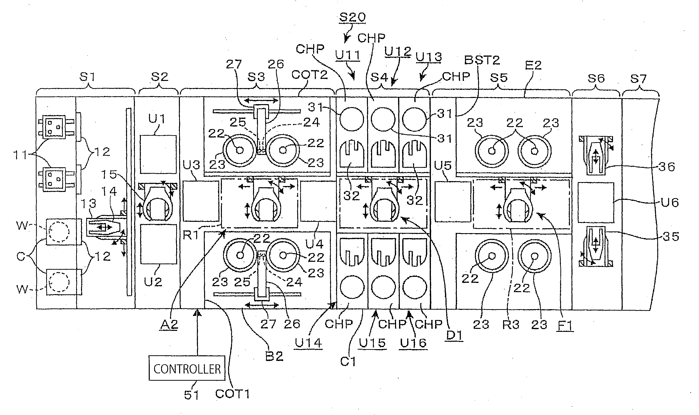
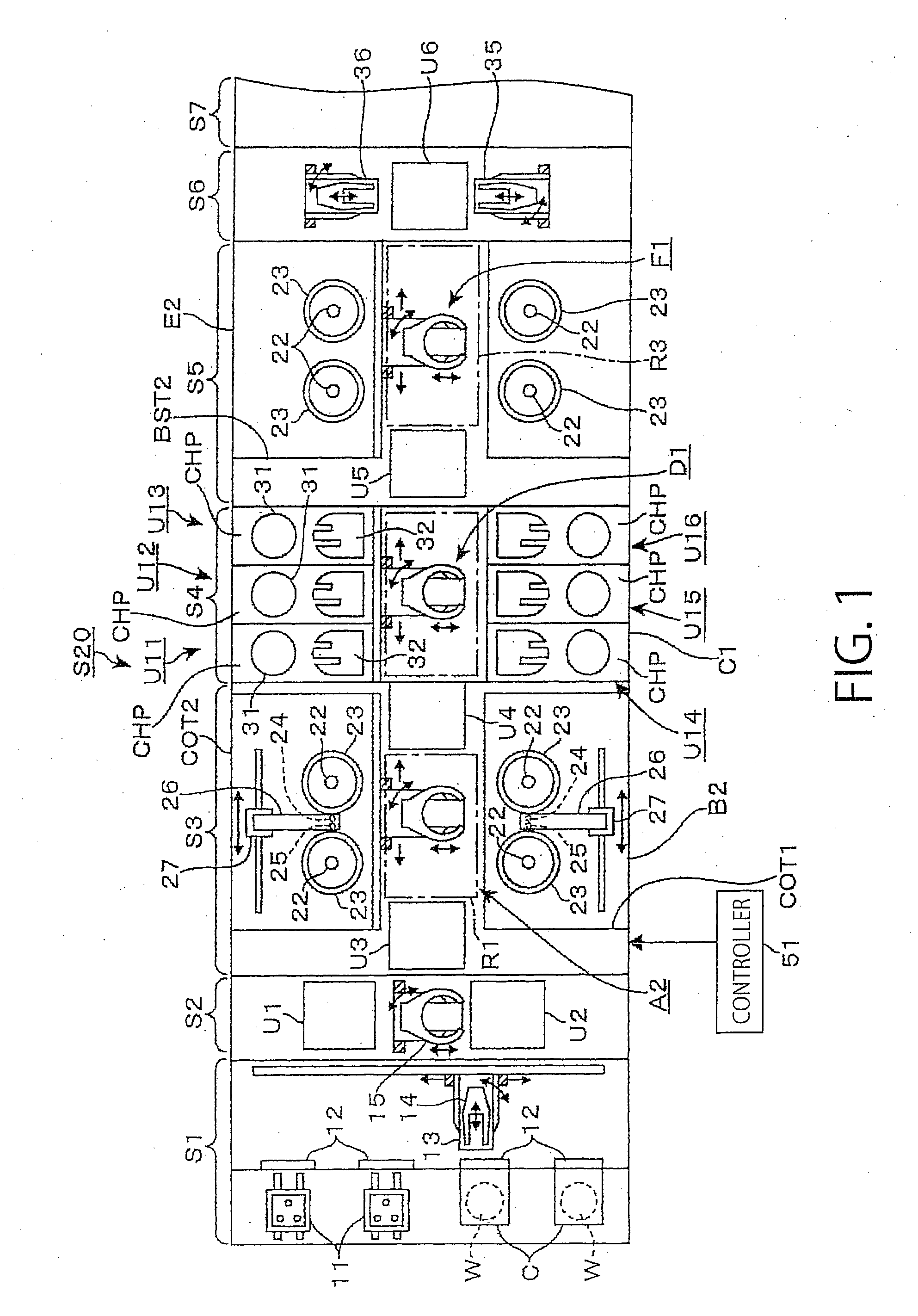
[0095]In the first embodiment described above and in the embodiments and the modifications described later, the timing at which the wafer W is subjected to the hydrophobizing process is not limited to that described above. For example, the transport route may be changed as follows: After formation of the resist film and the subsequent heating processing in the heating module PAB, the wafer may be transported through the main arm D1, the main arm A2 and the transfer module in the shelf unit U3 to one of the hydrophobizing modules ADH in the shelf units U1 and U2 in which the wafer W may be subjected to the hydrophobizing process. The wafer W may be then transported through the transfer module in the shelf unit U3 and the transfer arm 15 into the liquid processing block S2.

[0096]The coating and developing apparatus 1 in the foregoing embodiment includes the liquid processing block S3 which is formed by vertically stacking the liquid processing unit blocks B1 to B5 which are respective...

second embodiment

[0097

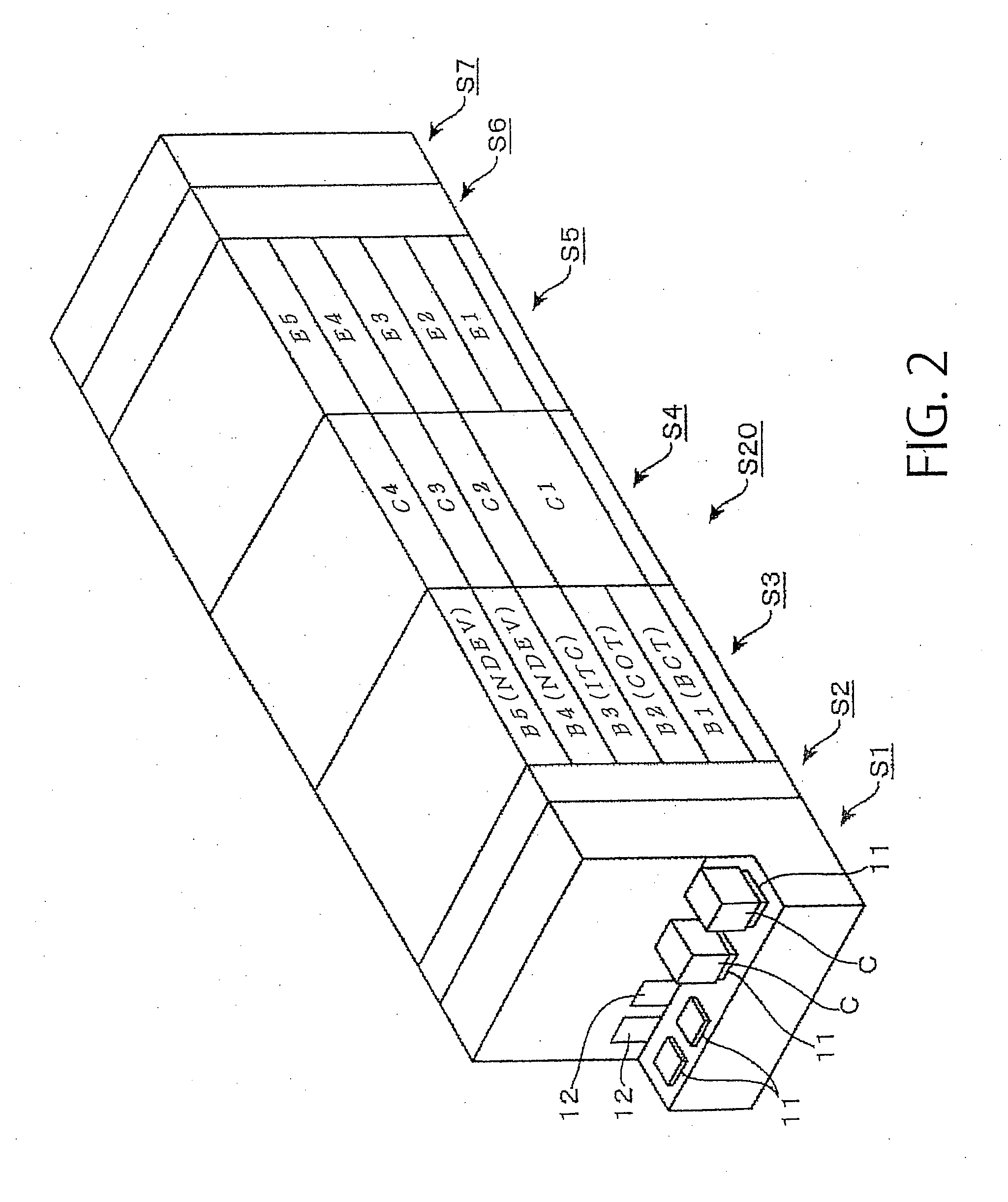
[0098]Next, a coating and developing apparatus 6 in a second embodiment will be described, focusing on the differences from the coating and developing apparatus 1. FIGS. 16, 17 and 18 are a plan view of the coating and developing apparatus 6, a perspective view thereof, and a vertical sectional side view thereof, respectively. As shown in FIG. 16, disposed in the anterior processing block S2 are a shelf unit U21 and a shelf unit U22 on the posterior side of the shelf unit U1 and the shelf unit U2, respectively. The space between the shelf unit U1 and the shelf unit U2, and the space between the shelf unit U21 and the shelf unit U22, provide a transport region R4 extending in the anteroposterior direction. The transfer arm 15 moves along the transport region R4 so as to transport wafers W to respective modules in the shelf units U1, U2, U21 and U22. FIG. 19 is a front view of the anterior processing block S2. Note that, for the convenience of the drawing making, the shelf units ...


PUM


Abstract

In one embodiment, a coating and developing apparatus is provided with a processing block including a liquid processing block disposed on the carrier block side and a heating processing block disposed on the interface block side. The liquid processing block includes a first unit block, a second unit block, and one or more of developing unit blocks overlying or underlying a stack of the first unit block and the second unit block. The first unit block includes antireflection film-forming modules and resist film-forming modules disposed on both sides of the transport passage thereof. The second unit block includes upper film-forming modules and hardening modules disposed on both sides of the transport passage thereof.

Description

CROSS-REFERENCE TO RELATED APPLICATION[0001]This application is based on and claims the benefit of priority to Japanese Patent Application No. 2010-197036 filed on Sep. 2, 2010, the entire contents of which are incorporated herein by reference.TECHNICAL FIELD[0002]The present disclosure relates to a coating and developing apparatus, a coating and developing method and a storage medium for applying a resist to a substrate and developing the resist after exposure.BACKGROUND ART[0003]A semiconductor manufacturing process includes a photolithography process comprising applying a photoresist (hereinafter simply referred to as a resist) to a surface of a semiconductor wafer (hereinafter simply referred to as a wafer), exposing the resist in a predetermined pattern, and developing the exposed resist to form a resist pattern. A coating and developing apparatus for forming such a resist pattern includes a processing block having processing modules for performing various types of processing o...

Claims


Application Information

Patent Timeline
IPC IPC(8): G03D5/04
CPCH01L21/6715H01L21/67178G03F7/3021G03F7/16H01L21/67184H01L21/0274H01L21/67721
Inventor MATSUOKA, NOBUAKIMIYATA, AKIRAHAYASHI, SHINICHIENOKIDA, SUGURU
Owner TOKYO ELECTRON LTD
Why Eureka
Try Eureka