Light emitting device and manufacturing method thereof

a technology of light emitting devices and manufacturing methods, which is applied in the direction of semiconductor devices for light sources, lighting and heating apparatus, point-like light sources, etc., can solve the problems of limited reflective efficiency of insulating paints, ineffective cost, and limited reflective efficiency of white plastic materials

Inactive Publication Date: 2012-03-29
ADVANCED OPTOELECTRONICS TECH
View PDF3 Cites 5 Cited by
  • Summary
  • Abstract
  • Description
  • Claims
  • Application Information

AI Technical Summary

Problems solved by technology

However, the reflective efficiency of the insulating paint is limited, having a reflective index of about 70˜80

Method used


Image

  • Light emitting device and manufacturing method thereof
  • Light emitting device and manufacturing method thereof
  • Light emitting device and manufacturing method thereof

Examples


Embodiment Construction

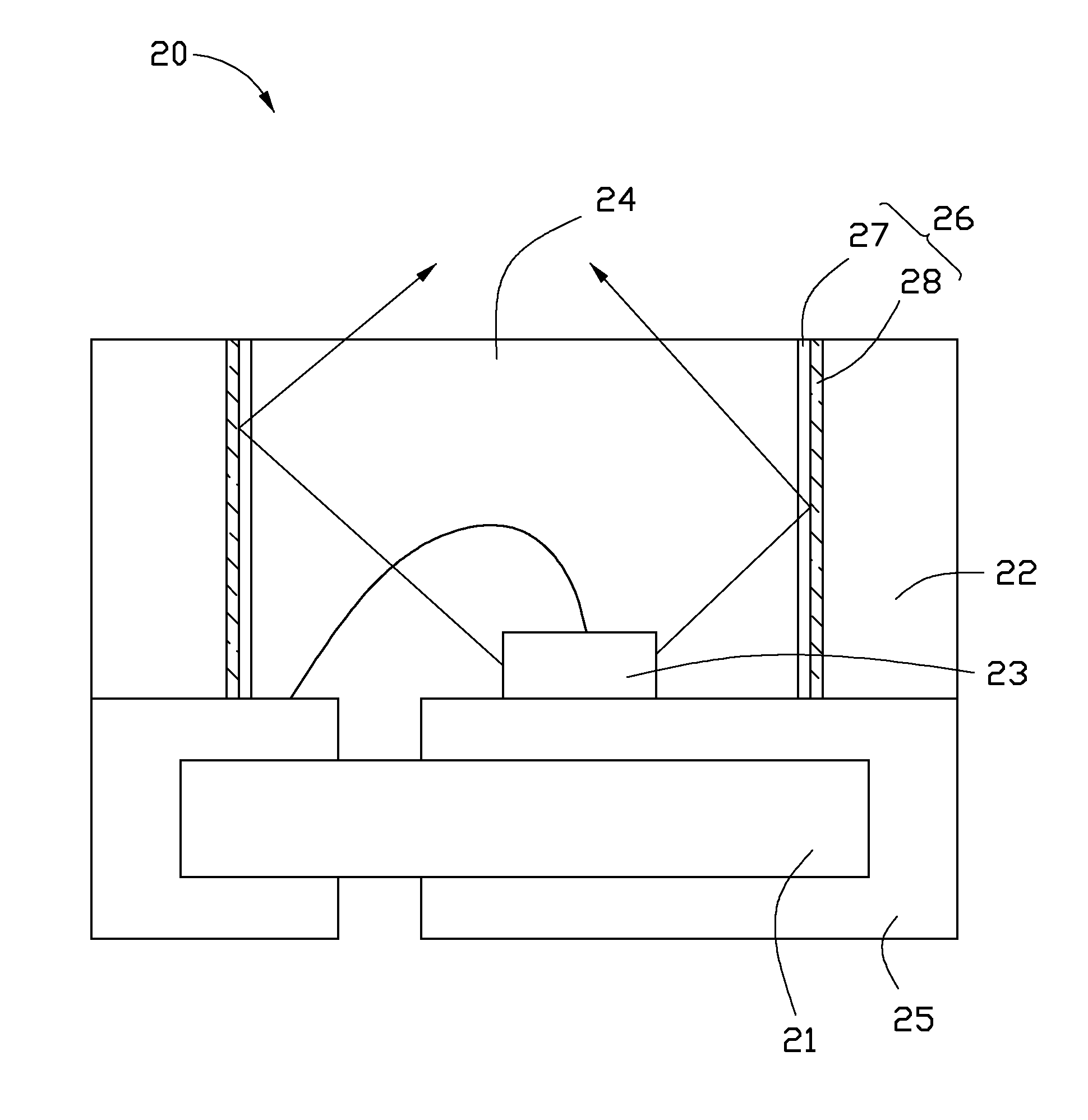
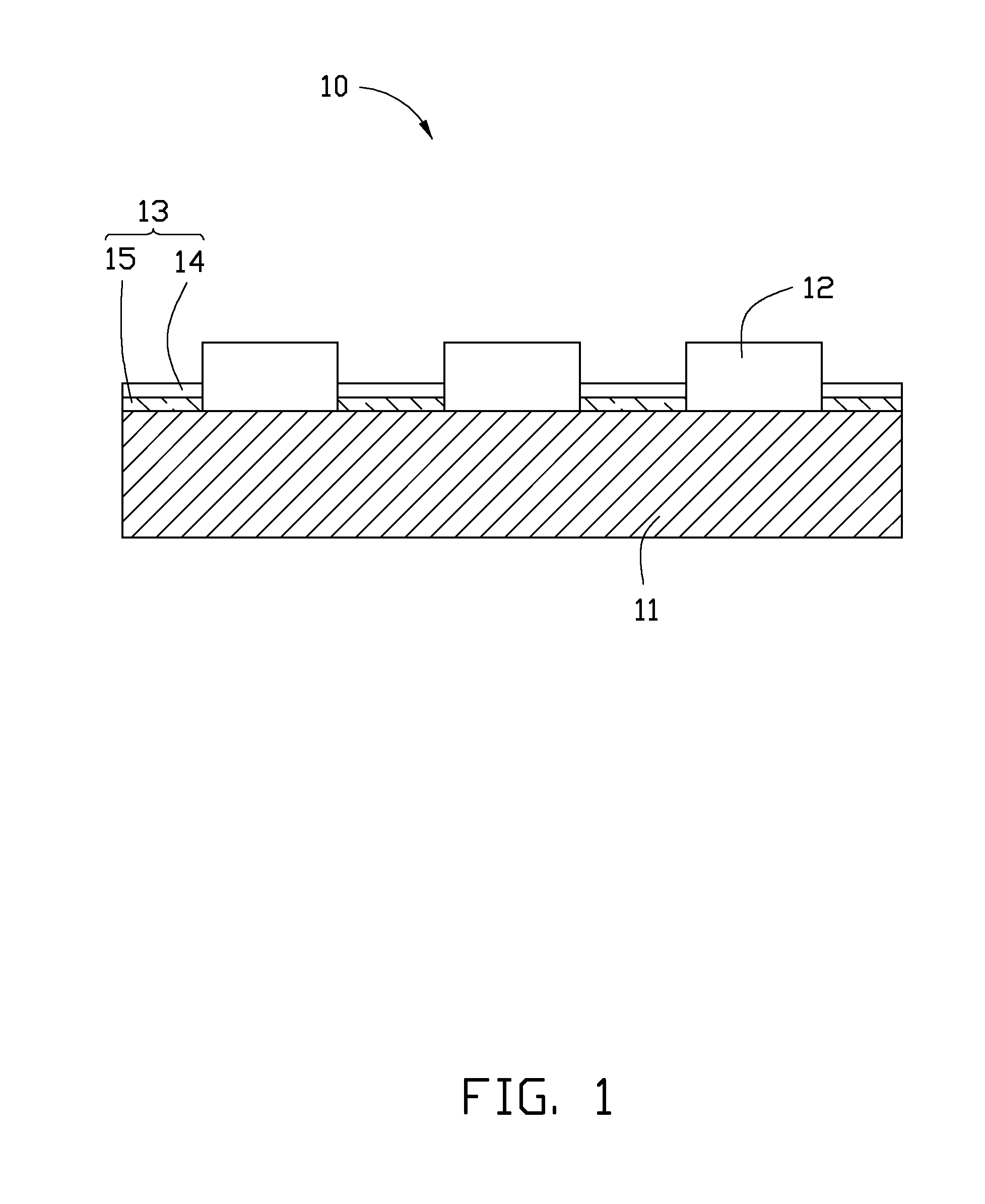
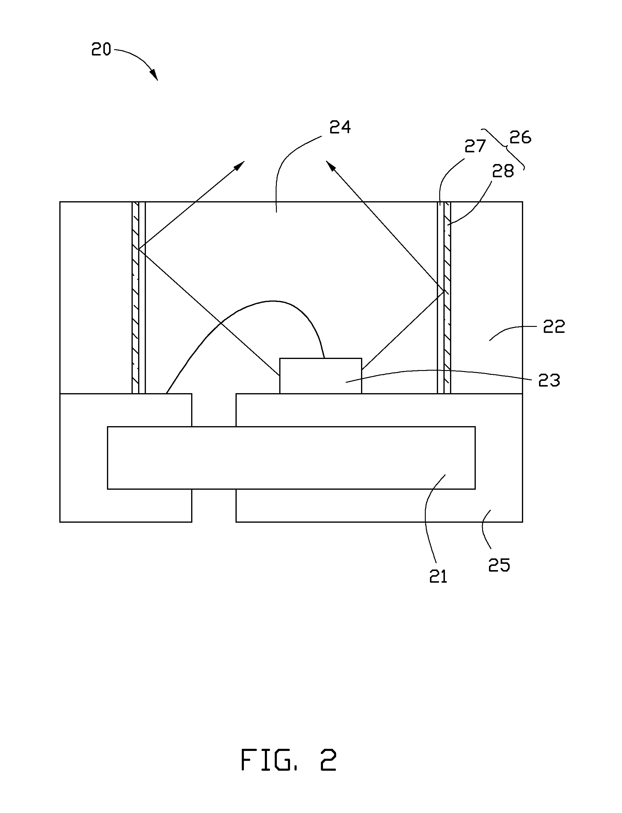
[0008]As shown in FIG. 1, the disclosure provides a light emitting module 10 comprising a printed circuit board (PCB) 11, a plurality of light emitting diodes (LEDs) 12 electrically connected to the PCB 11, and a reflector 13. Specifically, the light emitting diodes 12 and the reflector 13 are located on a top surface of the PCB 11, wherein the reflector 13 surrounds the LEDs 12.

[0009]The reflector 13 is composed of a transparent substrate 14 and a reflective material 15 applied to the transparent substrate 14 and located between the transparent substrate 14 and the PCB 11. The reflective material 15 comprises specular ink having high reflective index above 95%. Light reflected by the reflector 13 will have nearly its original illumination from the LEDs 12.

[0010]The specular ink is insulative, anti-oxidative and solder resistant. Accordingly, after the specular ink is dried, the specular ink is not liable to combine with other materials. That is, the circuitry of the light emitting ...


PUM

PropertyMeasurementUnit
Fractionaaaaaaaaaa
Transparencyaaaaaaaaaa
Water resistanceaaaaaaaaaa

Abstract

The disclosure provides a light emitting device comprising a light source and a reflector, having specular ink, surrounding the light source.

Description

TECHNICAL FIELD[0001]The disclosure relates generally to a light emitting device and a method for manufacturing the device, and more particularly to a semiconductor light emitting device and a method for manufacturing same.DESCRIPTION OF THE RELATED ART[0002]Presently, light emitting devices are widely used in lighting, which contain light emitting diode (LED) modules and light emitting diodes. Many light emitting diode modules include a printed circuit board (PCB) for providing electrical power to an LED light source. An insulating paint is applied on the exterior surface of the PCB to prevent short circuits. The insulating paint, usually white, is able to reflect light emitted from the LED light source. However, the reflective efficiency of the insulating paint is limited, having a reflective index of about 70˜80%, which is not cost effective.[0003]Similarly, the white plastic material is also widely used in the light emitting diodes to form a reflective cup or a reflector for ref...

Claims


Application Information

Patent Timeline
IPC IPC(8): H01L33/60
CPCF21K9/90F21V7/10F21V7/22F21Y2101/02H05K2201/2054H01L2933/0058H05K3/281H05K2201/10106H01L33/60H01L2224/48091F21Y2115/10F21V7/28H01L2924/00014
Inventor CHEN, YUE-ZHICHANG, CHIA-CHEN
Owner ADVANCED OPTOELECTRONICS TECH
Why Eureka
Try Eureka