

Voltage conversion module
a voltage conversion module and voltage conversion technology, applied in the direction of cross-talk/noise/interference reduction, printed electric component incorporation, printed circuit non-printed electric components association, etc., can solve the problem of not being able to obtain stable output voltage, capacitors, multi-layer wiring boards, etc., to achieve stable output voltage and reduce noise on input voltage.
- Summary
- Abstract
- Description
- Claims
- Application Information
AI Technical Summary
Benefits of technology
Problems solved by technology
Method used
Image

Examples
first embodiment
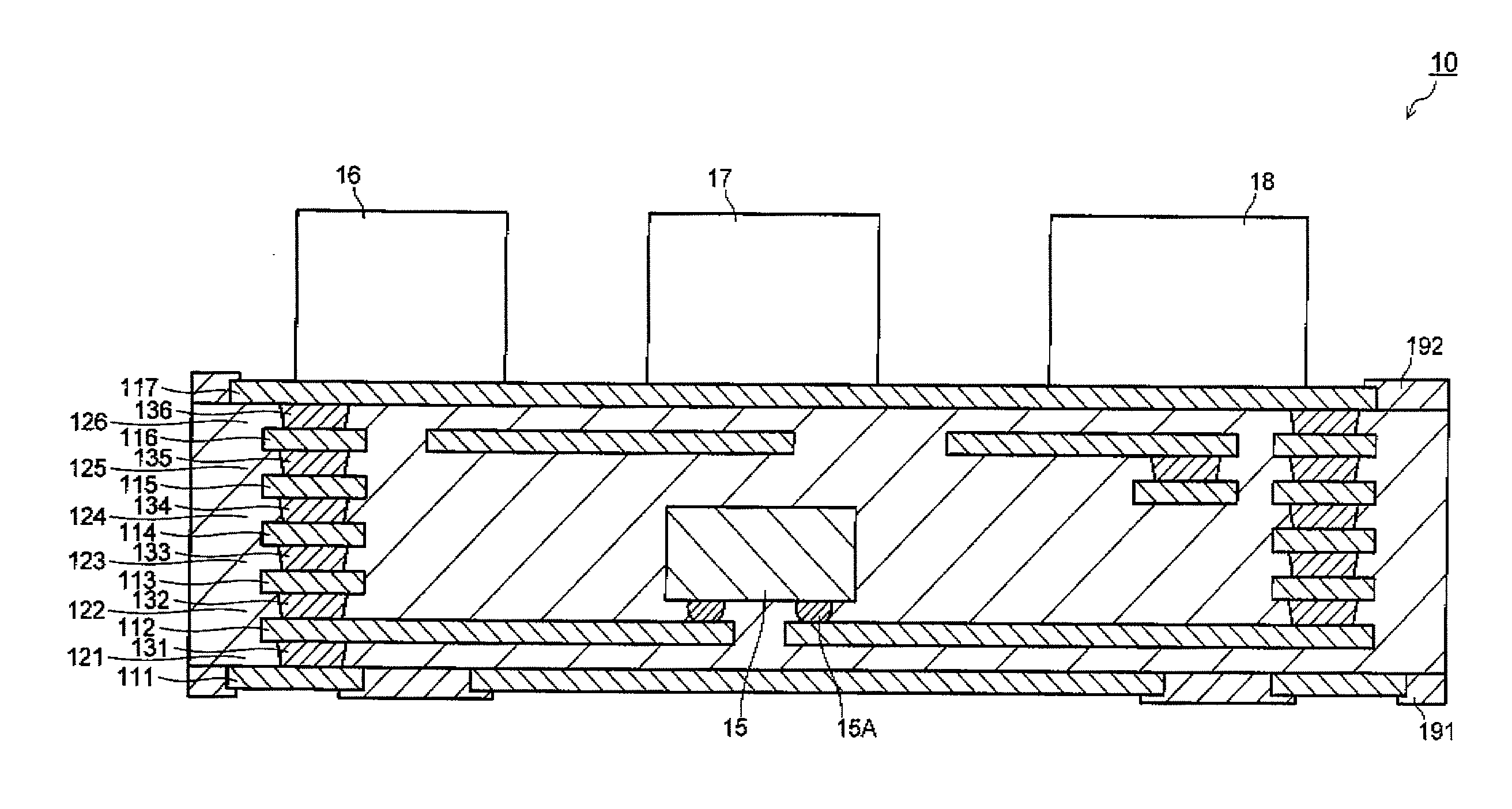
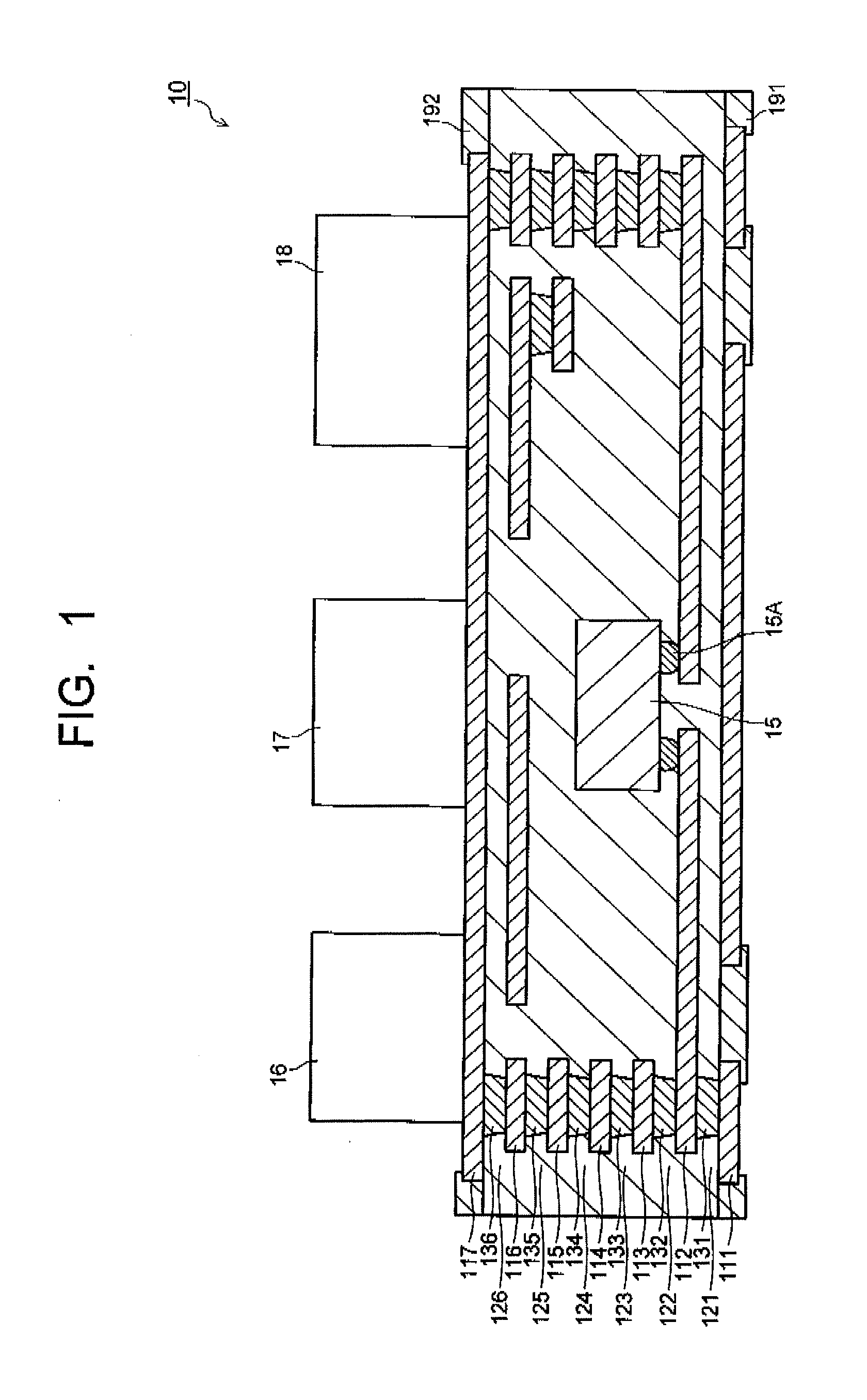
[0029]FIG. 1 is a partial cross-sectional configuration diagram illustrating a voltage conversion module of the present embodiment, while FIG. 2 is a top plan view of the voltage conversion module illustrated in FIG. 1. As is obvious from FIG. 1 and FIG. 2, only a portion of a multilayer wiring board of the voltage conversion module is illustrated in a cross section in FIG. 1.
[0030]A voltage conversion module 10 illustrated in FIG. 1 has, in sequence from a lower side, a first wiring pattern 111, a second wiring pattern 112, a third wiring pattern 113, a fourth wiring pattern 114, a fifth wiring pattern 115, a sixth wiring pattern 116, and a seventh wiring pattern 117.
[0031]Further, between the adjacent wiring patterns among the first wiring pattern 111 to the seventh wiring pattern 117, there are interposed a first insulating member 121 to a sixth insulating member 126, respectively.
[0032]More specifically, the first insulating member 121 exists between the first wiring pattern 111...
second embodiment
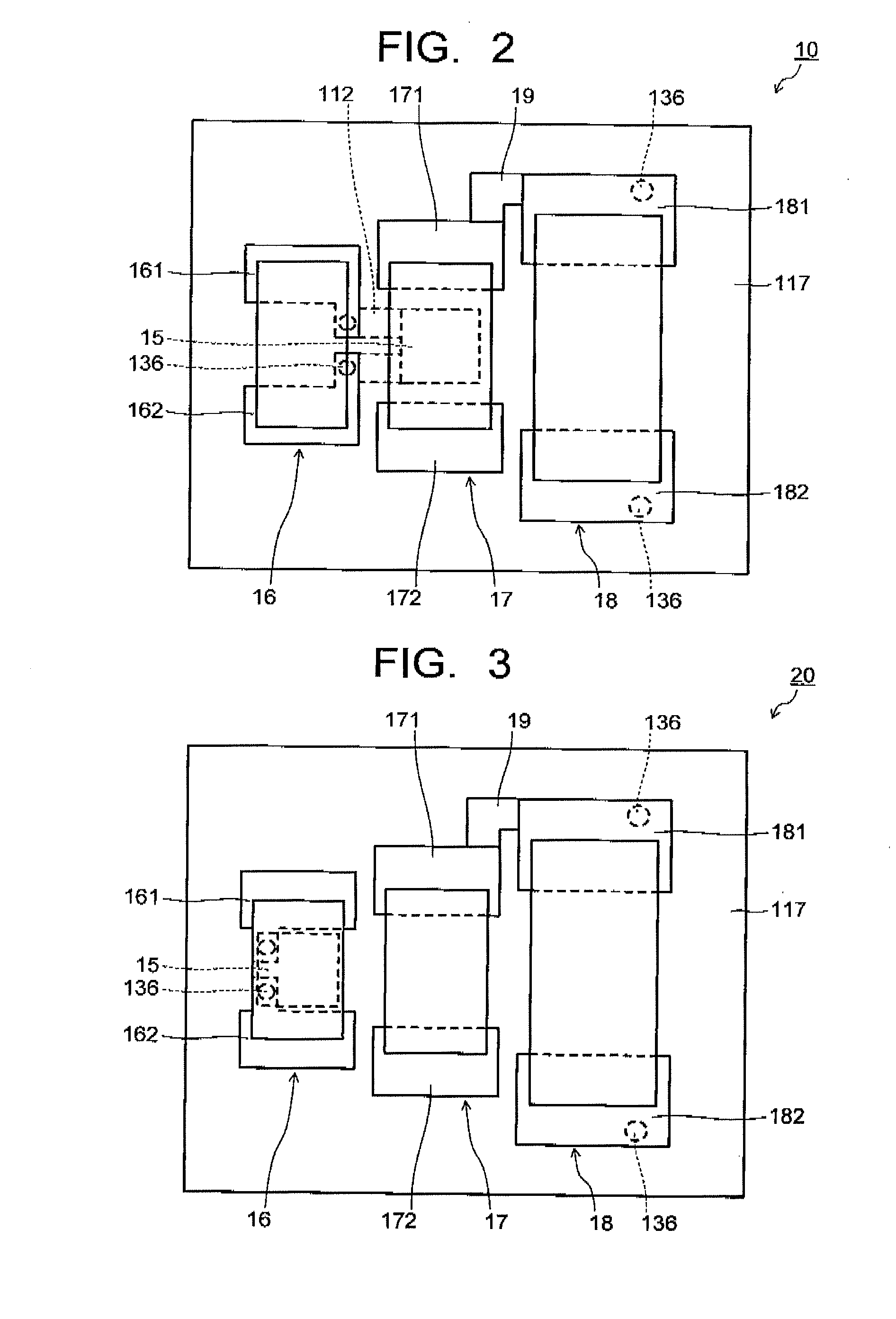
[0057]FIG. 3 is a top plan view illustrating an example of a voltage conversion module of the present embodiment. It should be noted that a component the same as or similar to the component illustrated in FIG. 1 and FIG. 2 related to the first embodiment is represented by using the same reference numeral.
[0058]As illustrated in FIG. 3, a voltage conversion module 20 of the present embodiment is configured such that a voltage conversion IC 15 is positioned, in a multilayer wiring board, directly below a first capacitor 16 mounted on the multilayer wiring board. In this case, since a length of a wiring connecting the voltage conversion IC 15 and the first capacitor 16 can be made shorter, an inductance value and a resistance value of the wiring can be reduced, so that the noise elimination of the voltage conversion IC 15 can be performed more effectively.
[0059]It should be noted that other features and configurations are the same as those of the first embodiment, and explanation there...
third embodiment
[0063]FIG. 4 is a partial cross-sectional configuration diagram illustrating an example of a voltage conversion module of the present embodiment, while FIG. 5 is a top plan view of the voltage conversion module illustrated in FIG. 4. As is obvious from FIG. 4 and FIG. 5, only a portion of a multilayer wiring board of the voltage conversion module is illustrated in a cross section in FIG. 4. It should be noted that a component the same as or similar to the component illustrated in FIG. 1 and FIG. 2 related to the first embodiment is represented by using the same reference numeral,
[0064]A voltage conversion module 30 illustrated in FIG. 4 has, similarly to the voltage conversion module 10 illustrated in FIG. 1, in sequence from a lower side, a first wiring pattern 111, a second wiring pattern 112, a third wiring pattern 113, a fourth wiring pattern 114, a fifth wiring pattern 115, a sixth wiring pattern 116, and a seventh wiring pattern 117. Further, between the adjacent wiring patter...
PUM
 Abstract
Description
Claims
Application Information