

Chip stacked structure
- Summary
- Abstract
- Description
- Claims
- Application Information
AI Technical Summary
Benefits of technology
Problems solved by technology
Method used
Image

Examples
first embodiment
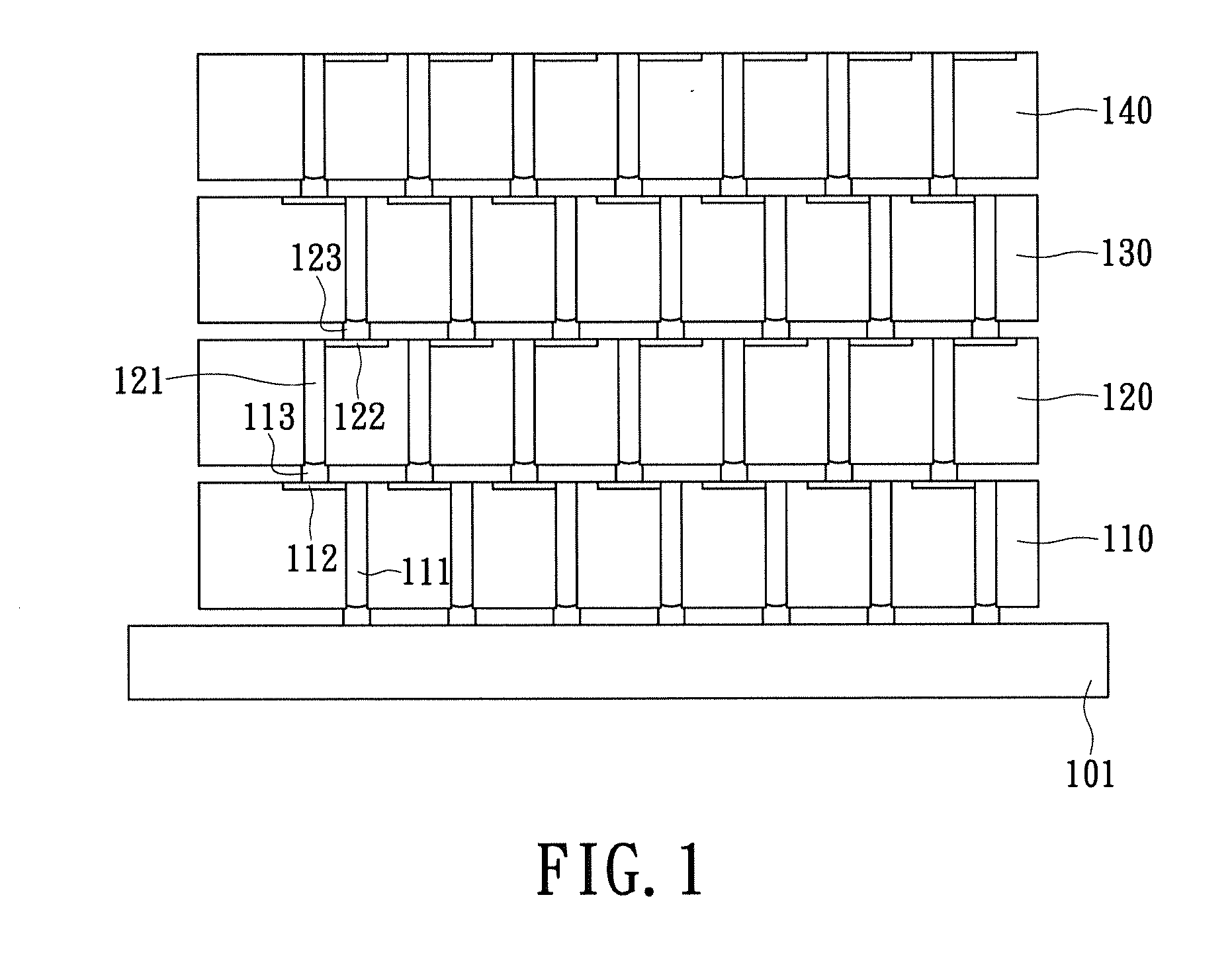
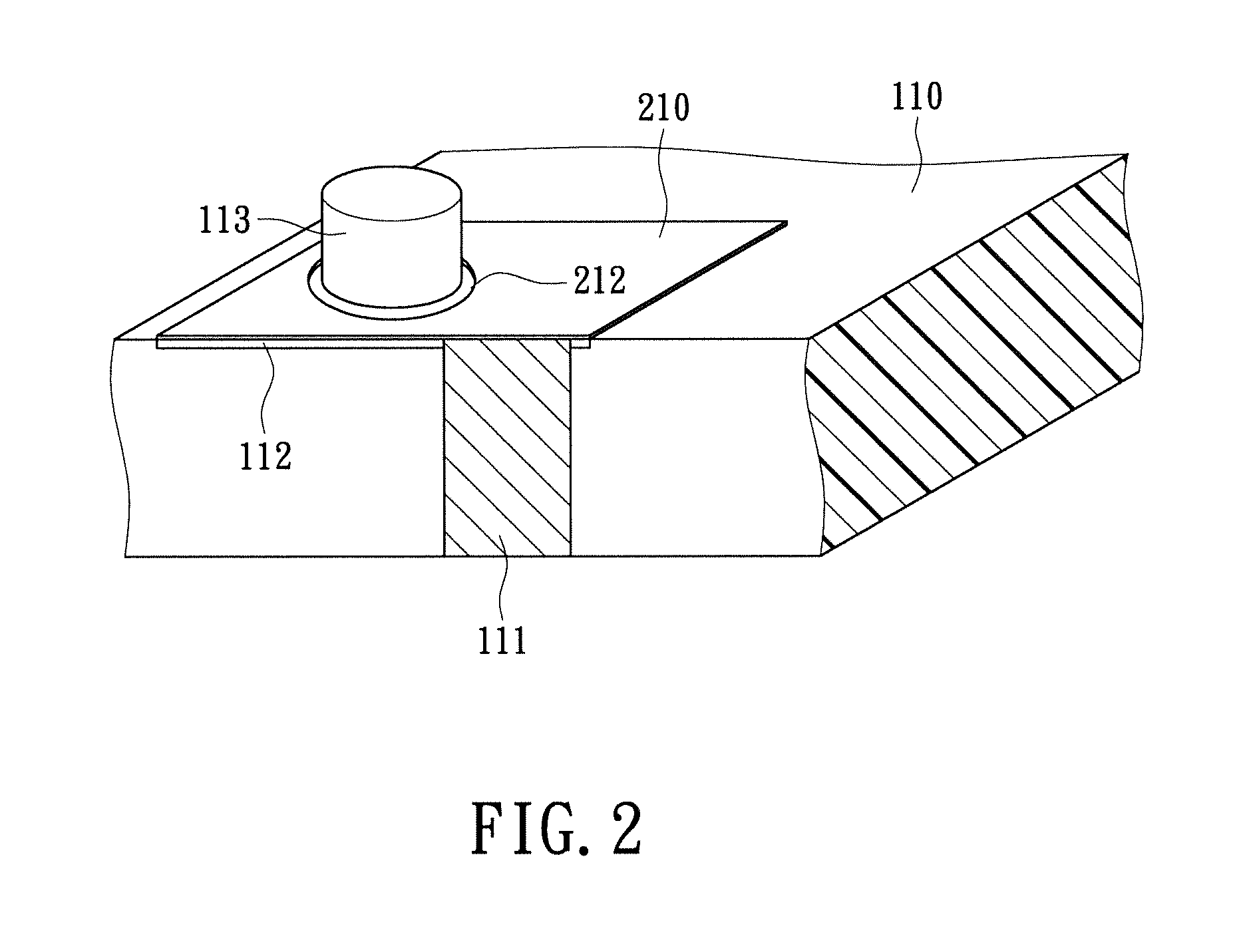
[0022]First of all, refer collectively to FIGS. 1 and 2, wherein FIG. 1 shows a diagram of the chip stacked structure according to a first embodiment of the present invention, and FIG. 2 shows a diagram of the connection structure according to the first embodiment of the present invention. The dies 110˜140 are disposed in a stack fashion, with each die comprising multiple connection structures for connecting to the die located in an upper layer. Taking the die 110 and 120 for example, the die 110 includes multiple connection structures, each connection structure having a through hole 111, a connection pad 112 and a solder bump 113 (also known as a solder ball). The through hole 111 is formed inside or on the edge of the die 110 by using the through-silicon via (TSV) technology, and the through hole 111 is filled with a conductive material thereby electrically connecting to the upper surface and lower surface of the die 110. The connection pad 112 is formed on the upper surface of th...
second embodiment
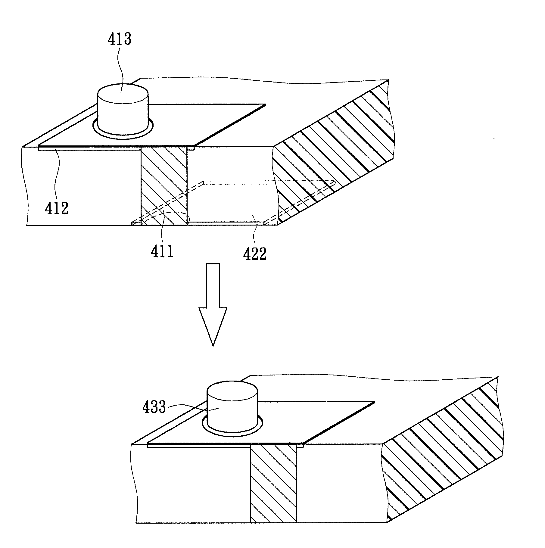
[0028]Refer now to FIG. 4, wherein a diagram of the connection structure according to a second embodiment of the present invention is shown. In FIG. 4, a connection pad 412 and 422 is respectively disposed on the upper and lower surfaces of the die, wherein the connection pad 412 is connected to the through hole 411 with the solder bump 413 installed thereon, while the connection pad 422 is connected to the other end of the through hole 411. Since the connection pad 422 has a larger area, it is hence more convenient to align in position to the solder bump 433 disposed on the lower die thereby elevating the process yield rate and alignment precision. The connection structure shown in FIG. 4 can be directly applied on the dies 110˜140 described in FIG. 1 so as to simplify the manufacture process and increase the process yield rate. Through the aforementioned descriptions on the present embodiment, those skilled ones in the art are capable of inferring to other possible implementations...
PUM
 Abstract
Description
Claims
Application Information