Coil on a semiconductor substrate and method for its production

Inactive Publication Date: 2005-05-05
INFINEON TECH AG
View PDF6 Cites 22 Cited by
  • Summary
  • Abstract
  • Description
  • Claims
  • Application Information

AI Technical Summary

Benefits of technology

[0027] A further advantage of the present invention is the fact that the coil means may be produced at low cost and efficiently with standard processes of semiconductor production, and/or that the inventive production process may be carried out with standard processes and may therefore be integrated into semiconductor production in a simple and straightforward manner.
[0028] A further advantage is the fact that the resonance-vibration frequency range may be raised due to the clearly reduced parasitic capacitances. This leads to a considerable expansion of the spectrum of possible uses of an inventive coil means and/or of a coil produced in

Problems solved by technology

However, in many cases the dopant of the silicon substrate cannot be chosen freely since it typically is linked, at the same time, to other properties of the silicon substrate, for example to its suitability for certain devices or arrangements of devices.
However, this typically involves a fair amount of work and considerable extra cost

Method used


Image

  • Coil on a semiconductor substrate and method for its production
  • Coil on a semiconductor substrate and method for its production
  • Coil on a semiconductor substrate and method for its production

Examples


first embodiment

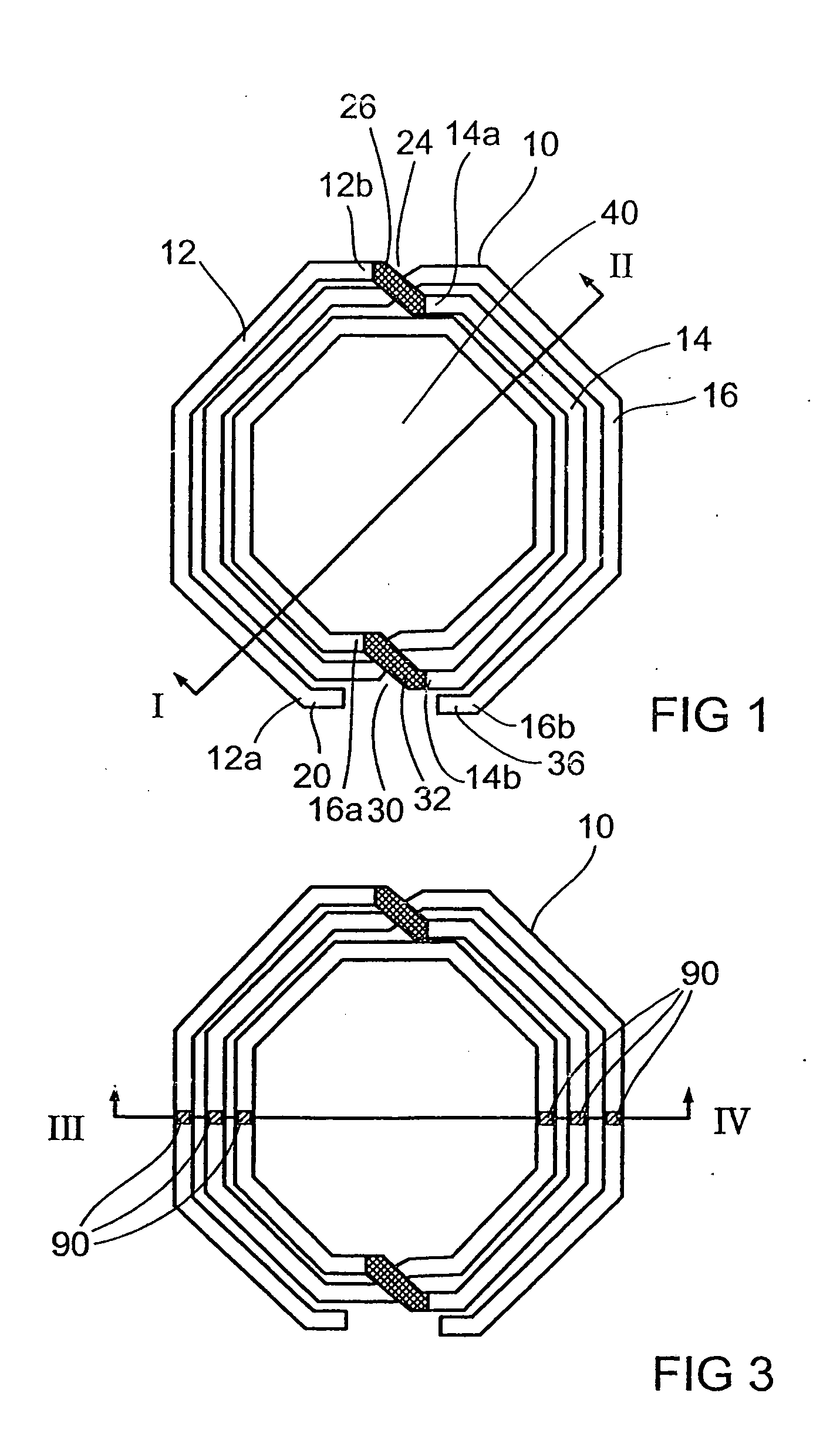
[0040]FIG. 1 is a schematic top view of a coil in accordance with the present invention. The coil is formed by a coil trace 10 with several sections 12, 14, 16 which are arranged concentrically to one another approximately in the form of sub-sections of regular octagons. The first section 12 of the coil trace 10 includes a first contacting area 20 at a first end 12a. A second end 12b of the first section is connected to a first end 14a of the second section in an electrically conductive manner via a first connector piece 26 in a first crossing area 24, the first connector piece 26 crossing the third section 16 and being electrically insulated from same by an insulating layer (not shown). A second end 14b of the second section 14 is connected, via a second connector piece 32, to a first end 16a of the third section 16 in an electrically conductive manner in a second crossing area 30, the second connector piece 32 crossing the third section 16 and being electrically insulated from sam...

third embodiment

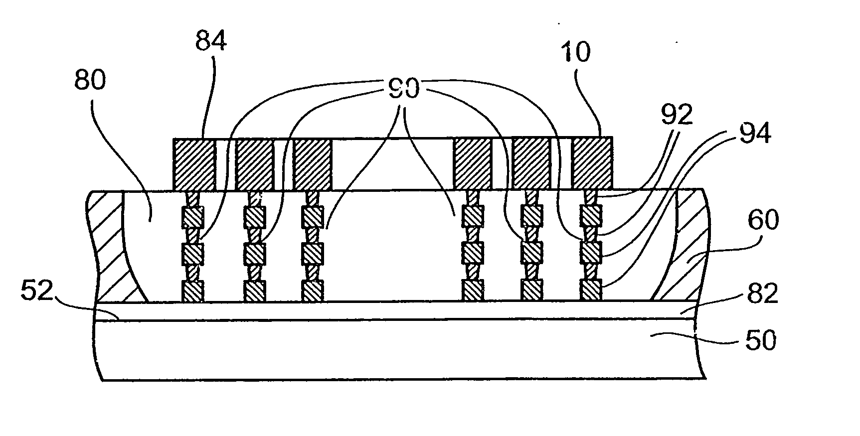
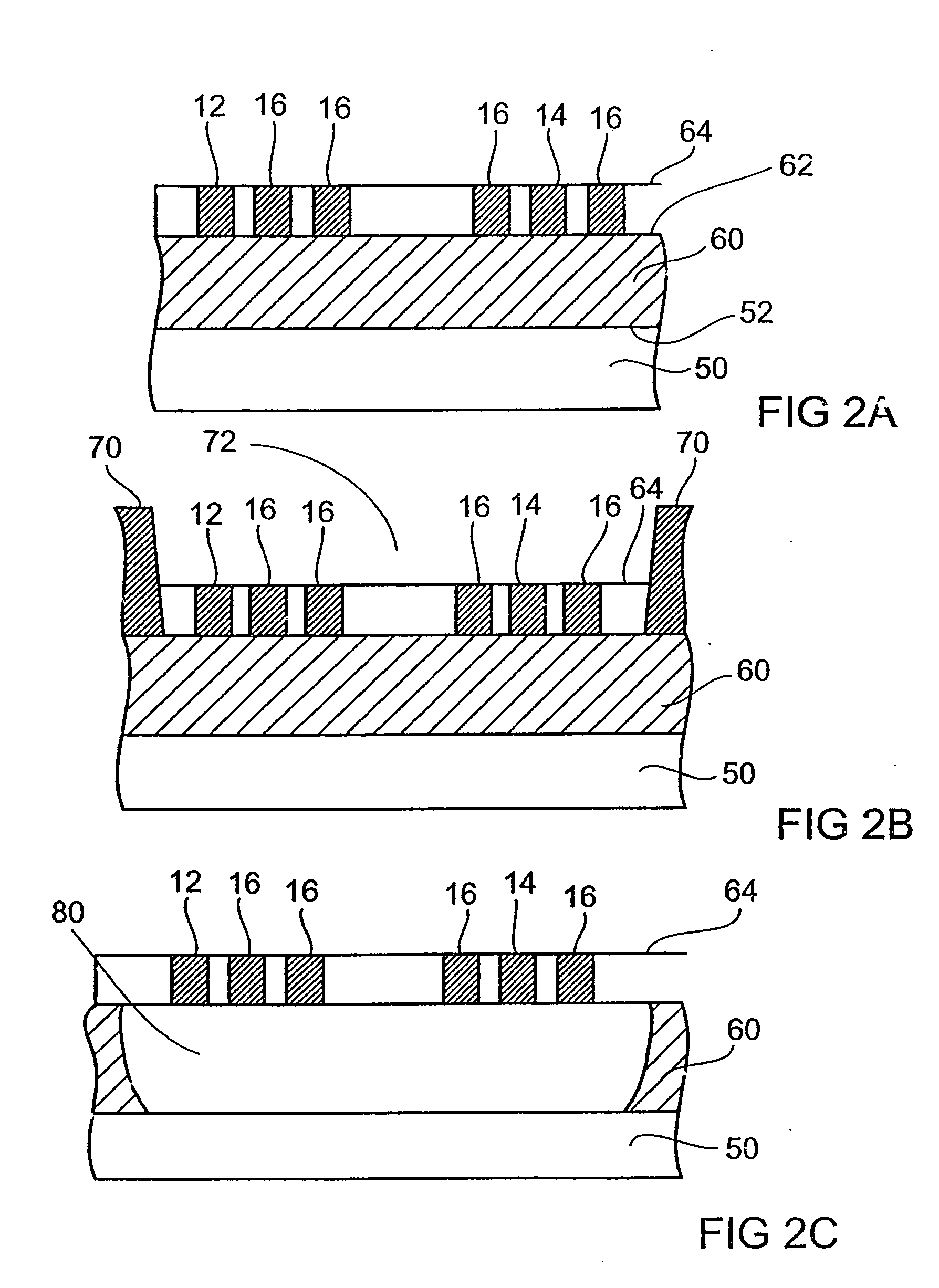
[0056] In the third embodiment, a passivation sheathing, or passivation layer, 84 is further represented, which has already been shown in FIG. 4 but has a larger thickness of layer here.

[0057]FIG. 5B shows a schematic representation of a section through a coil means in accordance with a fourth embodiment. This embodiment differs from the first embodiment in that a supporting layer 102 is provided on the coil trace 10, the supporting layer 102 comprising, in the form of an aperture mask for producing the recess 80, holes 104 through which an etching medium creating the recess 80 may pass. The supporting layer 102 has a mechanical support function and thus improves mechanical stability of the coil trace 10. Instead of the passiviation layer 84 sheathing the coil trace 10, as is shown in FIGS. 4 and 5A, a passivation layer 106 is provided on the support layer 102, the thickness of the passivation layer 106 preferably being selected such that the holes 104 of the supporting layer 102 ar...


PUM

PropertyMeasurementUnit
Thicknessaaaaaaaaaa
Electrical conductoraaaaaaaaaa
Areaaaaaaaaaaa

Abstract

A coil apparatus includes a coil trace, a semiconductor substrate and a dielectric layer arranged on the semiconductor substrate, at least parts of the coil trace being arranged above a recess in the dielectric layer. The coil apparatus further includes a support apparatus arranged in the recess and connected to the coil trace for mechanically supporting the coil trace. The supporting apparatus is preferably a conductive column that is not removed when the recessed is formed in the dielectric layer.

Description

CROSS-REFERENCE TO RELATED APPLICATION [0001] This application is a continuation of co-pending International Application No. PCT / EP03 / 02880, filed Mar. 19, 2003, which designated the United States and was not published in English and is incorporated herein by reference in its entirety.BACKGROUND OF THE INVENTION [0002] 1. Field of the Invention [0003] The present invention relates to a coil on a semiconductor substrate, in particular to a high-quality coil, and to a method of producing same. [0004] 2. Description of the Related Art [0005] Many integrated semiconductor packages and / or semiconductor chips contain coils. When producing a semiconductor package, a device layer having a plurality of diodes, transistors or other semiconductor devices is created on the surface of a silicon substrate. Several layers of wiring which contain metallic wiring conductor tracks for wiring the devices and in addition may contain capacitors, coils etc., are created above the device layer. [0006] Ele...

Claims


Application Information

Patent Timeline
IPC IPC(8): H01F17/00H01F41/04H01L21/02H01L23/522H01L27/08
CPCH01F41/041H01F2017/0046H01L23/5227H01L27/08Y10T29/4902H01L2924/0002H01L28/10H01L2924/00
Inventor BUEYUEKTAS, KEVNIKOLLER, KLAUSMUELLER, KARLHEINZ
Owner INFINEON TECH AG
Why Eureka
Try Eureka