Laser irradiation apparatus, laser irradiation method, and method for manufacturing a semiconductor device

Active Publication Date: 2011-04-05
SEMICON ENERGY LAB CO LTD
View PDF56 Cites 3 Cited by
  • Summary
  • Abstract
  • Description
  • Claims
  • Application Information

AI Technical Summary

Benefits of technology

According to the present invention, the absorption coefficient of the fundamental wave to the semiconductor film is increased by irradiating the first laser beam having a wavelength of visible light or a shorter wavelength than that of visible light to melt the semiconductor film. By irradiating the first pulsed laser beam, the area of the beam spot can be enlarged than that when irradiated by the CW laser beam. And by irradiating the second laser beam having a fundamental wave to the melted semiconductor film, the second laser beam is absorbed effectively in the semiconductor film in which the absorption coefficient of the fundamental wave is increased. As a result, since the major axis of the beam spot can be made long, throughput of the laser crystallization can be enhanced and it is effective to ease the design rule.
It is noted that the region which is melted by the first laser beam and in which the absorption coefficient is increased can be moved by scanning the second laser beam and thereby the region where the crystal grains

Problems solved by technology

It is a problem that when a carrier is trapped in the trapping center, potential of the crystal grain boundary increases to become a barrier against the carrier, and thereby deteriorating a carrier mobility.
Therefore it is difficult to enhance throughput by enlarging the area of the beam spot.
Especially, since the output energy from the CW laser oscillator p

Method used


Image

  • Laser irradiation apparatus, laser irradiation method, and method for manufacturing a semiconductor device
  • Laser irradiation apparatus, laser irradiation method, and method for manufacturing a semiconductor device
  • Laser irradiation apparatus, laser irradiation method, and method for manufacturing a semiconductor device

Examples


embodiment mode 1

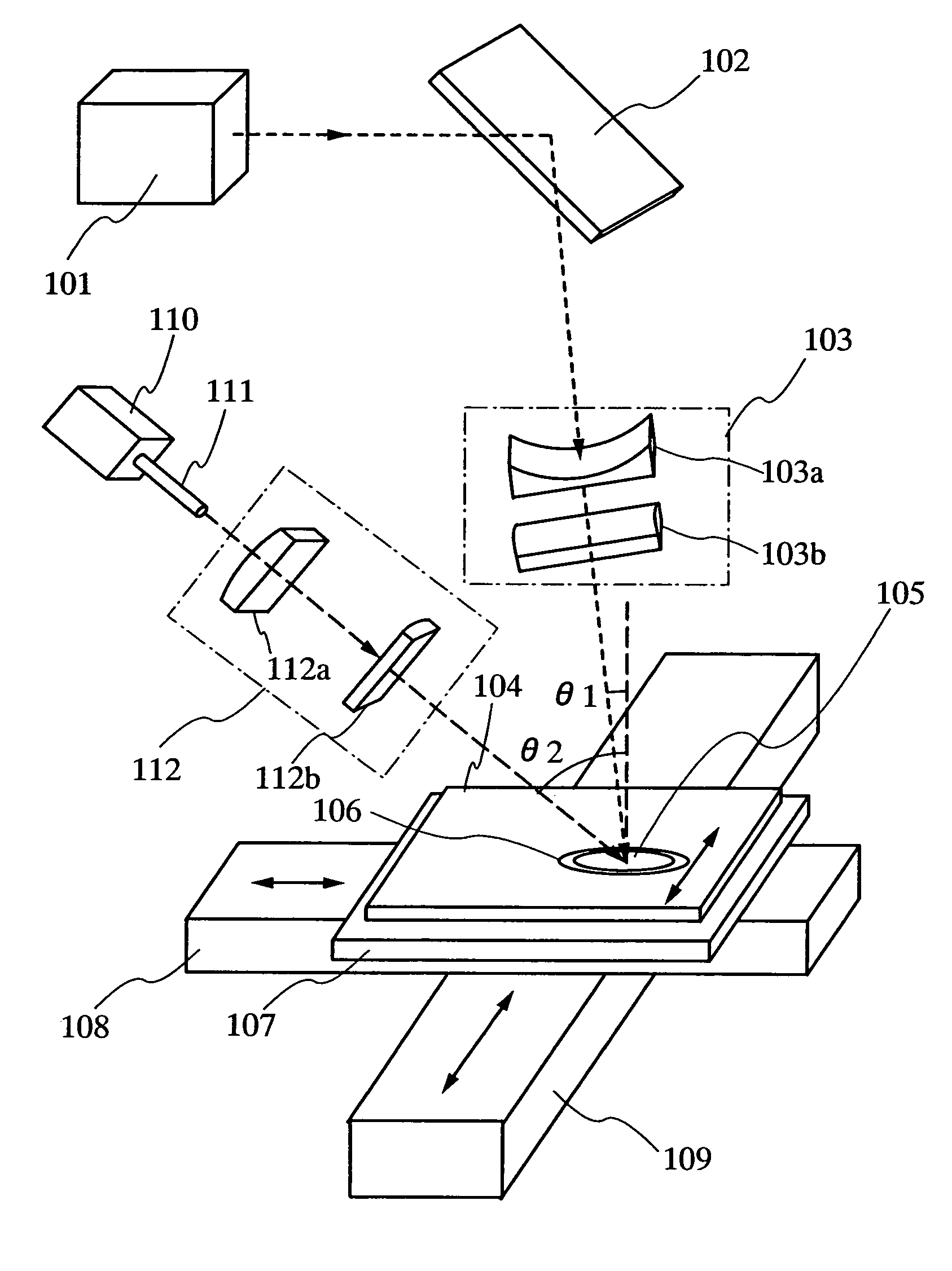
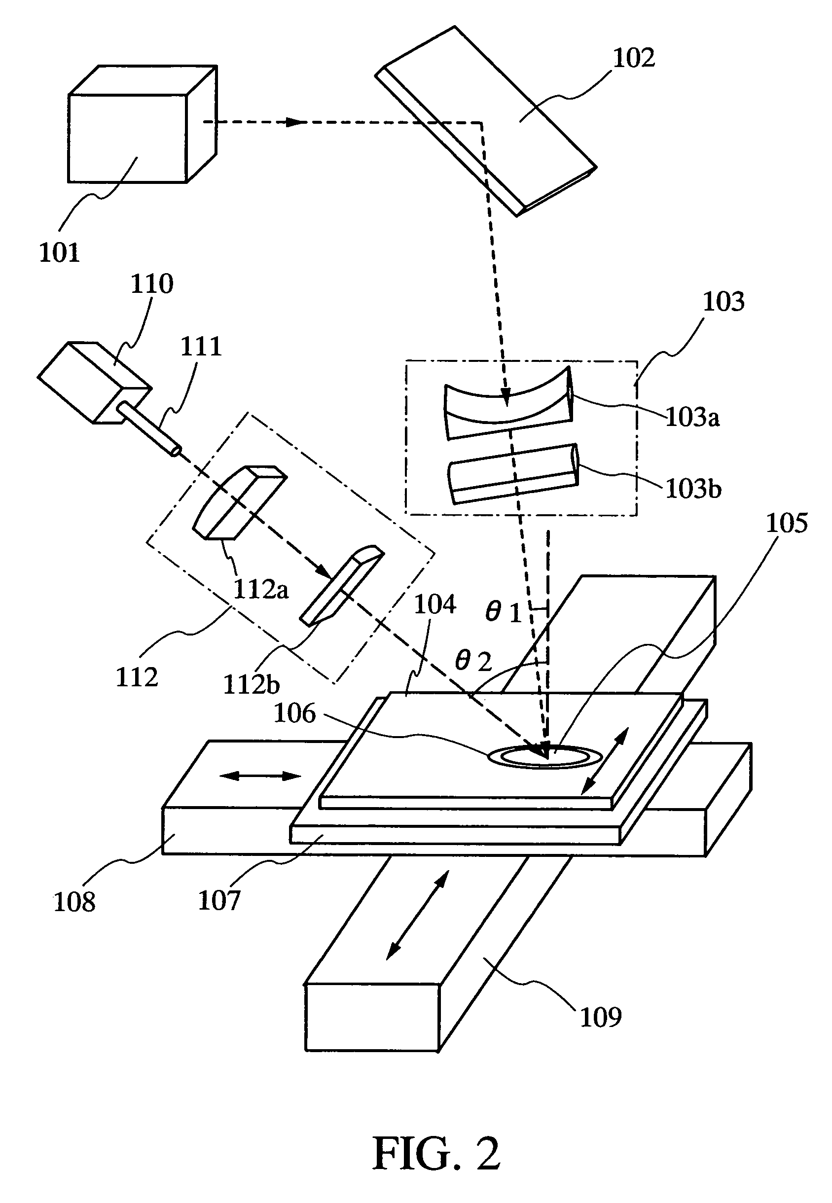
The structure of the laser irradiation apparatus according to the present invention is explained with using FIG. 2.

Reference numeral 101 denotes a pulsed laser oscillator, and a Nd: YLF laser that outputs 6 W is used as the laser oscillator 101 in this embodiment mode. The laser oscillator 101 operates in a TEM00 mode and includes the non-linear optical element to convert the wavelength of the laser beam into the second harmonic. The higher harmonic is also available but the second harmonic is superior in terms of the energy efficiency to the other higher harmonics. The frequency is 1 kHz and the pulse width is 60 ns approximately. In this embodiment mode, the solid laser that outputs 6 W approximately is used but a large-scaled laser oscillator that outputs as much as 300 W, for example aXeCl excimer laser, can be also employed.

It is noted that the non-linear optical element may be provided inside the resonator included in the oscillator or the resonator equipped the non-linear opt...

embodiment mode 2

In this embodiment mode, the method for irradiating a laser beam and the method for manufacturing a semiconductor device according to the present invention is explained with FIGS. 4A to 4C.

First of all, a base film 501 is formed on a substrate 500 as shown in FIG. 4A. A glass substrate such as a barium borosilicate glass, an aluminum borosilicate glass or the like, a quartz substrate, an SUS substrate or the like can be given as the substrate 500. Besides, though the substrate comprising the plastic typically polyethilene terephthalate (PET), polyethersulfone (PES), and polyethylene naphthalate (PEN) or acryl synthetic-resin with flexibility such as acryl or the like is inferior to the substrate above in terms of the resistance against the heat, it can be utilized provided that the substrate can resist against the heat generated in the manufacturing processes.

The base film 501 is provided in order to prevent that alkaline-earth metal or alkaline metal such as Na comprised in the sub...

embodiment 1

This embodiment shows one example of the laser irradiation apparatus applying the present invention.

FIG. 5 shows a structure of the laser irradiation apparatus in this embodiment. In this embodiment, a first pulsed laser beam having a wavelength of visible light or a shorter wavelength than that of visible is emitted from a laser oscillator 1520. And second CW laser beams are emitted from two laser oscillators 1500 and 1501.

In this embodiment, an excimer laser is used as the laser oscillator 1520, which outputs the energy of 1 J per a pulse, with a pulse width of 30 ns approximately, that is to say the laser oscillators 1520 outputs 30 MW per unit time. In addition, both of the laser oscillators 1500 and 1501 are YAG lasers which output 10 kW respectively.

After the first laser beam emitted from the laser oscillator 1520 is reflected by the mirror 1523, the first laser beam is shaped into rectangular, elliptical or linear through the optical system 1524 and is irradiated to the proce...


PUM

PropertyMeasurementUnit
Wavelengthaaaaaaaaaa

Abstract

It is an object to provide a laser irradiation apparatus for enlarging an area of a beam spot and reducing a proportion of a region with low crystallinity. It is also an object to provide a laser irradiation apparatus for enhancing throughput with a CW laser beam. Furthermore, it is an object to provide a laser irradiation method and a method for manufacturing a semiconductor device with the laser irradiation apparatus. A region melted by a first pulsed laser beam having harmonic is irradiated with a second CW laser beam. Specifically, the first laser beam has a wavelength of visible light or a shorter wavelength than that of visible light (approximately not more than 830 nm, preferably, not more than 780 nm). Since the first laser beam melts a semiconductor film, an absorption coefficient of the second laser beam to the semiconductor film increases drastically and thereby being more absorbable.

Description

BACKGROUND OF THE INVENTION1. Field of the InventionThe present invention relates to a laser irradiation apparatus utilized for crystallizing a semiconductor film. Moreover, the present invention relates to a laser irradiation method and a method for manufacturing a semiconductor device using the laser irradiation apparatus of the present invention.2. Description of the Related ArtThin film transistor employing poly-crystalline semiconductor film (poly-crystalline TFT) is superior by double digits or more to TFT employing an amorphous semiconductor film in terms of its mobility, and thereby has an advantage that a pixel portion and a peripheral driver circuit thereof in a semiconductor display device can be integrated on a same substrate. The poly-crystalline semiconductor film can be formed over an inexpensive glass substrate by employing a laser annealing method.Laser oscillators are generally classified into two types of pulsed laser oscillators and continuous wave (CW) laser osc...

Claims


Application Information

Patent Timeline
IPC IPC(8): B23K26/00G03B27/48H01S3/10
CPCB23K26/0732G03B27/48B23K26/0738B23K26/0736H01S3/10
Inventor TANAKA, KOICHIRO
Owner SEMICON ENERGY LAB CO LTD
Why Eureka
Try Eureka