Thin film transistor and display device using the same

Active Publication Date: 2012-04-26
SAMSUNG DISPLAY CO LTD
View PDF9 Cites 27 Cited by
  • Summary
  • Abstract
  • Description
  • Claims
  • Application Information

AI Technical Summary

Benefits of technology

[0010]An aspect of an embodiment of the present invention is directed toward a thin film transistor that

Problems solved by technology

However, the crystallization method using a laser beam has a problem in that a crystallization protrusion is formed at the surface of a polycrystalline silicon film crystallized through t

Method used


Image

  • Thin film transistor and display device using the same
  • Thin film transistor and display device using the same
  • Thin film transistor and display device using the same

Examples


Embodiment Construction

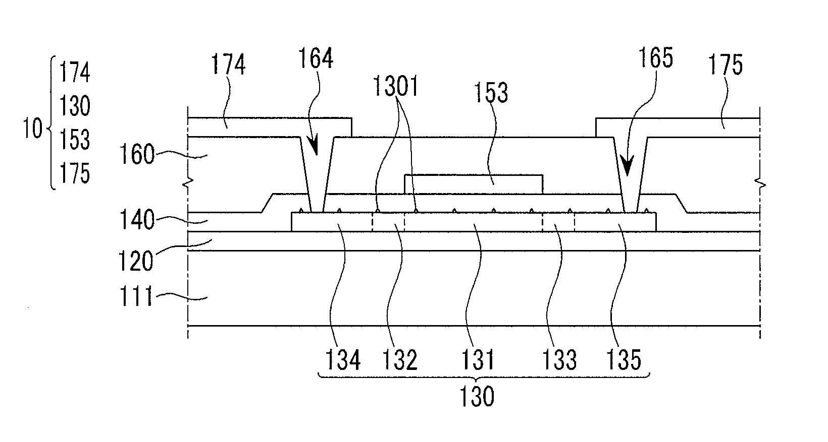
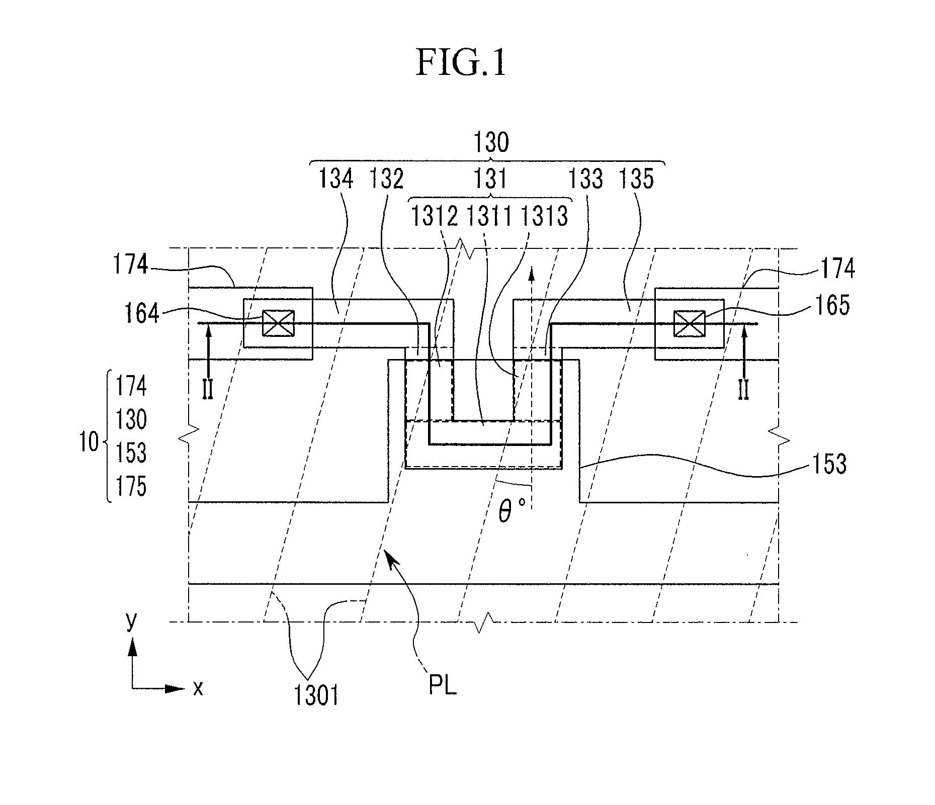
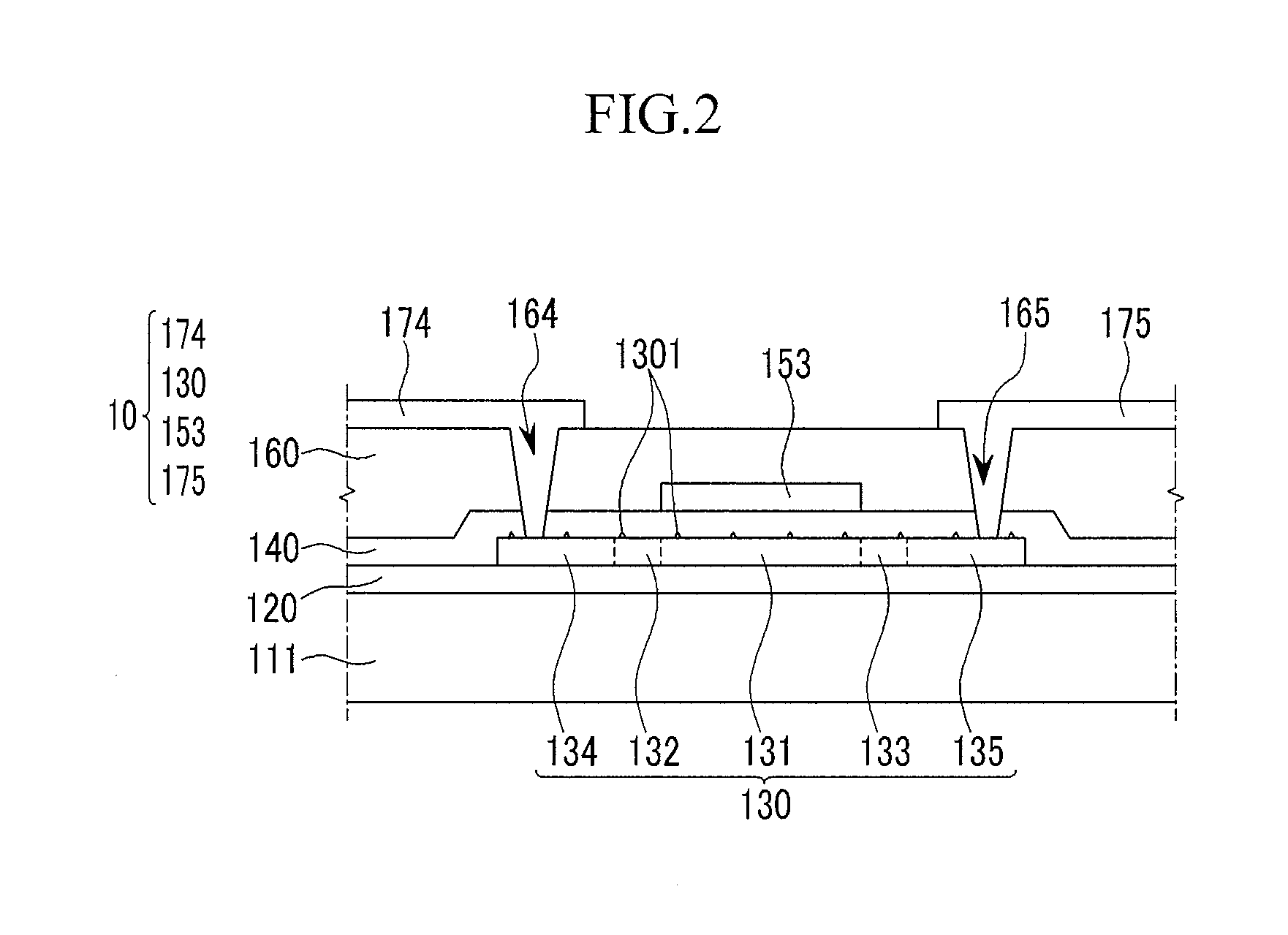
[0029]The present invention will be described more fully hereinafter with reference to the accompanying drawings, in which exemplary embodiments of the invention are shown. As those skilled in the art would realize, the described embodiments may be modified in various different ways, all without departing from the spirit or scope of the present invention.

[0030]Constituent elements having the same structures throughout the embodiments are denoted by the same reference numerals and are described in a first exemplary embodiment.

[0031]Furthermore, as the size and thickness of the respective structural components shown in the drawings are arbitrarily illustrated for explanatory convenience, the present invention is not necessarily limited to the illustrated. In the drawings, for better understanding and ease of description, the thickness of layers, films, panels, regions, etc., are exaggerated for clarity. It will be understood that when an element such as a layer, film, region, or subst...


PUM


Abstract

In a thin film transistor and a display device provided with the same, a thin film transistor according to an exemplary embodiment includes: a semiconductor layer including a channel region, a source region, a drain region, a light-doped source region, and a light-doped drain region; a gate electrode overlapping the channel region; a source electrode contacting the source region; and a drain electrode contacting the drain region. The channel region includes a main channel portion, a source channel portion, and a drain channel portion, and the source channel portion and the drain channel portion are extended from the main channel portion and separated from each other. The light-doped source region is disposed between the source channel portion and the source region and the light-doped drain region is disposed between the drain channel portion and the drain region.

Description

CROSS-REFERENCE TO RELATED APPLICATION[0001]This application claims priority to and the benefit of Korean Patent Application No. 10-2010-0103498, filed in the Korean Intellectual Property Office on Oct. 22, 2010, the entire content of which is incorporated herein by reference.BACKGROUND[0002]1. Field[0003]The following description relates generally to a thin film transistor and a display device having the same. More particularly, the described technology relates generally to a thin film transistor that can suppress occurrence of a failure due to a crystallization protrusion formed in a semiconductor layer, and a display device having the same.[0004]2. Description of Related Art[0005]Most flat panel display devices, such as an organic light emitting diode (OLED) display, a liquid crystal display (LCD), and the like, include a thin film transistor. Particularly, a low temperature polycrystalline silicon thin film transistor (LTPS TFT) having good carrier mobility can be applicable to ...

Claims


Application Information

Patent Timeline
IPC IPC(8): H01L29/786
CPCH01L27/1285H01L29/78696H01L29/78621H01L29/34
Inventor SHIN, JAE-MINPARK, JI-YONGPARK, KYUNG-MIN
Owner SAMSUNG DISPLAY CO LTD
Why Eureka
Try Eureka