Image display device

a display device and image technology, applied in static indicating devices, instruments, transportation and packaging, etc., can solve the problems of not being able to verify whether or not only the wavelength shift caused by temperature is compensated by the input, and the disclosed technologies in patent document 3 are also problematic in terms of cos

Inactive Publication Date: 2012-04-26
PANASONIC CORP
View PDF6 Cites 38 Cited by
  • Summary
  • Abstract
  • Description
  • Claims
  • Application Information

AI Technical Summary

Benefits of technology

[0013]It is an object of the present invention to provide an image display device for displaying quality images.

Problems solved by technology

The disclosed technologies in the aforementioned Patent Documents 1 and 2 contain problems about control under actual usage conditions.
Therefore, it is difficult to suppress variations in the emission spectrum and prevent the central wavelength of the emission spectrum from shifting.
Therefore, it has not been verified whether or not only the wavelength shift caused by temperature is compensated by the input current.
Therefore, the disclosed technologies in Patent Document 3 are also problematic in terms of cost.Patent Document 1: JP 2008-102442 APatent Document 2: JP 2009-99701 APatent Document 3: JP 2007-226190 A

Method used


Image

  • Image display device
  • Image display device
  • Image display device

Examples


first embodiment

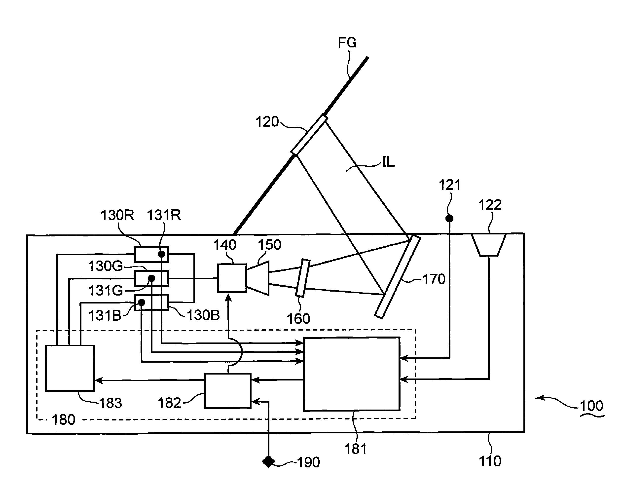
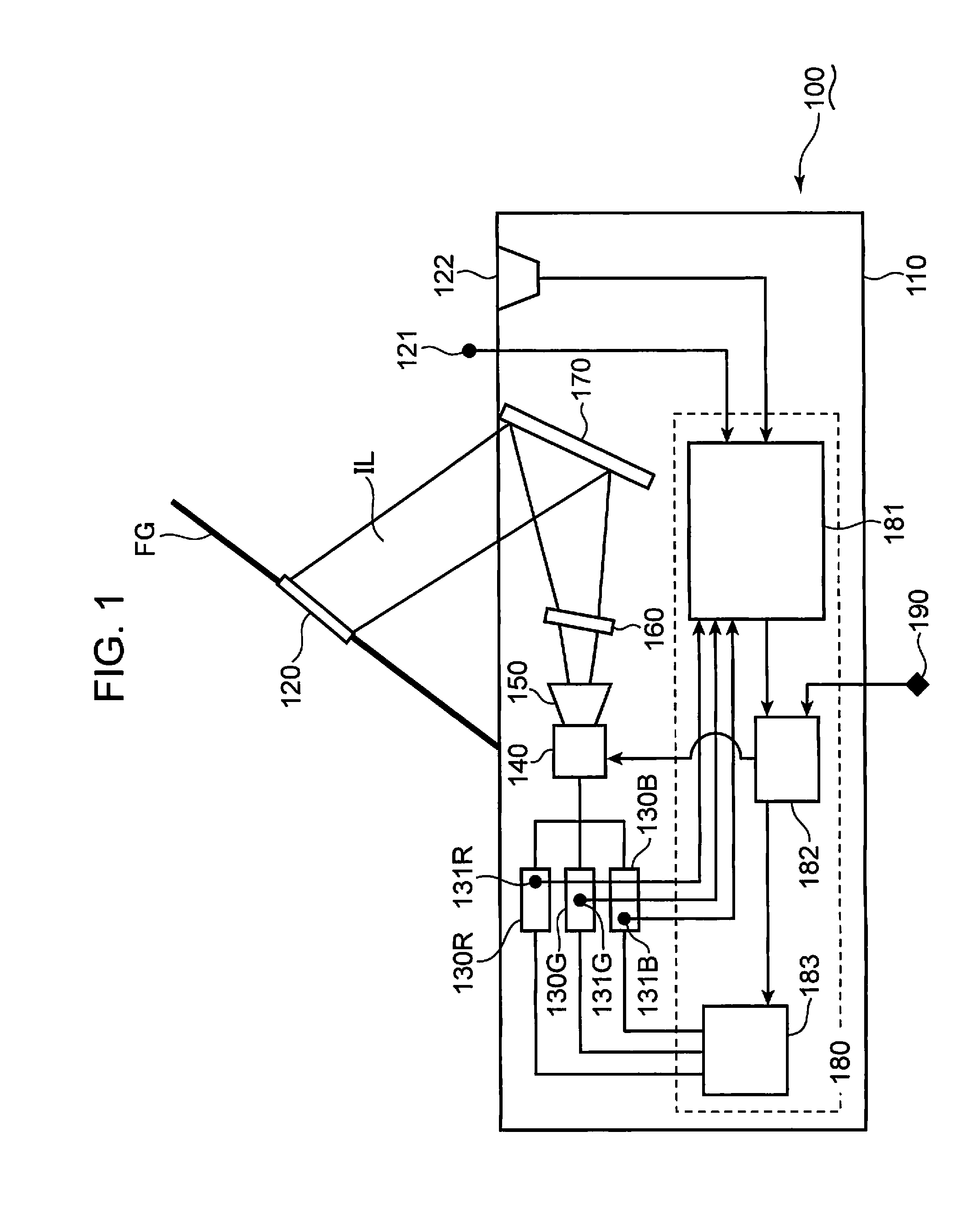
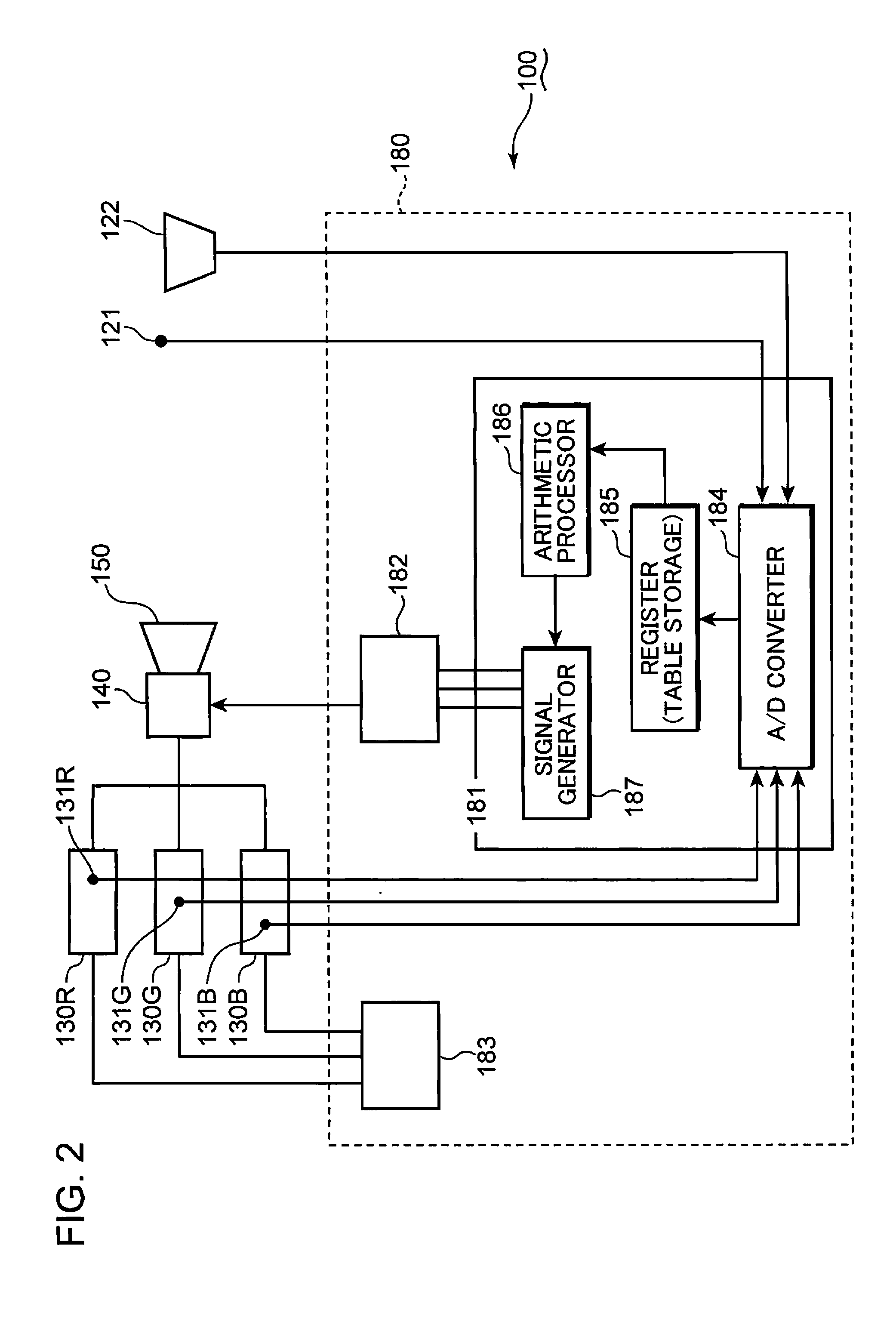
[0046]In the first embodiment, a head-up display device is exemplified as the image display device. According to the principles of the first embodiment, a temperature of a hologram optical element is predicted in response to the temperature around the hologram optical element and a quantity of external light falling around the hologram optical element. The temperatures of laser sources are monitored to predict the central wavelengths of the laser beams emitted from the laser sources. A suitable diffraction angle at which a diffraction efficiency of the hologram optical element becomes the highest is calculated in response to the predicted temperature of the hologram optical element and the predicted central wavelength of the laser beam. A display position of the image formed by the image forming unit is adjusted in response to the calculated value of the diffraction angle, so that a driver perceives little degradation of the viewed image.

[0047]FIG. 1 is a schematic view of an interi...

second embodiment

[0090]In the second embodiment, the temperature of the hologram optical element is measured by a hologram pattern formed in a hologram optical element region, which does not contribute to image display. The temperature of the hologram optical element is determined in response to positions of laser beams diffracted by the hologram pattern formed for measuring the temperature in order to identify the shift amount of the displayed image.

[0091]FIG. 5 is a schematic view of a head-up display device exemplified as the image display device according to the second embodiment. The head-up display device according to the second embodiment is described with reference to FIG. 5.

[0092]The head-up display device 100A according to the present embodiment is provided with a hologram optical element 120A which is attached to the windshield FG and a main body 110A which emits image light IL onto the hologram optical element 120A. The hologram optical element 120A is provided with a first hologram 125 ...


PUM


Abstract

An image display device includes a laser source for emitting a laser beam, an image forming element which uses the laser beam to emit image light for displaying an image, a first diffraction element for diffracting the image light, and a controller for controlling a display position of the image on the basis of a wavelength of the laser beam and a temperature of the first diffraction element.

Description

TECHNICAL FIELD[0001]The present invention is related to an image display device for forming an image by means of a laser beam generated by a laser source.BACKGROUND OF THE INVENTION[0002]There are various proposed image display devices configured to display an image by means of laser beams generated by laser sources such as laser diodes. An electronic printing device (laser printer or copier), which scans a beam to form an image, is exemplified as the image display device. A photo-plotter, which directly irradiates recording paper with red, green and blue laser beams to burn-in a photo, is exemplified as another image display device. A projector, which irradiates a screen, instead of the aforementioned recording paper, with red, green and blue laser beams in order to display an image, is exemplified as yet another image display device. Another projector, which is used as an image display device, irradiates a two-dimensional modulator such as an ultra-small liquid crystal element or...

Claims


Application Information

Patent Timeline
Patent Type & Authority Applications(United States)
IPC IPC(8): G06F3/038
CPCG02B5/18G02B5/32G02B26/10B60K2350/2052G02B2027/0112B60K35/00G02B27/0101B60K2370/334
Inventor FURUYA, HIROYUKISHIKII, SHINICHISUGIYAMA, KEIJI
Owner PANASONIC CORP
Why Eureka
Try Eureka