Pixel structure and fabricating method thereof

a technology of pixel structure and fabricating method, which is applied in the direction of non-linear optics, instruments, radio frequency controlled devices, etc., can solve the problems of waste of energy, and achieve the effect of superb display quality and higher aperture ratio

Inactive Publication Date: 2012-04-24
CHUNGHWA PICTURE TUBES LTD
View PDF1 Cites 3 Cited by
  • Summary
  • Abstract
  • Description
  • Claims
  • Application Information

AI Technical Summary

Benefits of technology

[0011]The invention provides a pixel structure having a higher aperture ratio and superb display quality.
[0012]The invention provides a fabricating method of a pixel structure and increasing production yield.
[0032]In light of the above, in the pixel structure of the invention, the common line is designed to partially overlap with the data line, so that the aperture ratio of the pixel structure is increased. Moreover, the common electrode which is electrically connected with the common line is formed on the common line, so that the electrical field formed between the common electrode and the pixel electrode drives the liquid crystals. Hence the pixel structure provides a wide viewing angle. Furthermore, since the common line and the scan line are not fabricated by the same photomask process, occurrence of a short circuit between the common line and the scan line is prevented, thereby increasing the production yield and enabling the pixel structure to have superb display quality.

Problems solved by technology

Therefore, to maintain the brightness of the pixel structure 100, it is necessary to add light sources in the display device, which is a waste of energy.

Method used


Image

  • Pixel structure and fabricating method thereof
  • Pixel structure and fabricating method thereof
  • Pixel structure and fabricating method thereof

Examples


Embodiment Construction

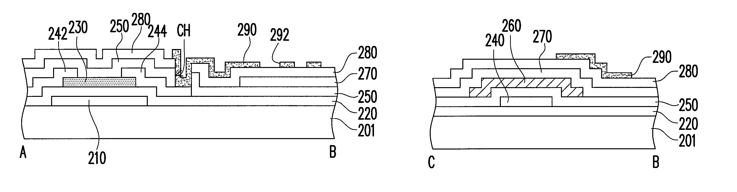
[0039]In the invention, a number of photomask processes is increased, so that a loss of an aperture ratio caused by disposition of a common electrode is prevented. A pixel structure having a high aperture ratio and superb display quality is thereby fabricated. Particularly, since the common line and a scan line are not formed by the same photomask process, occurrence of a short circuit between the common line and the scan line is prevented.

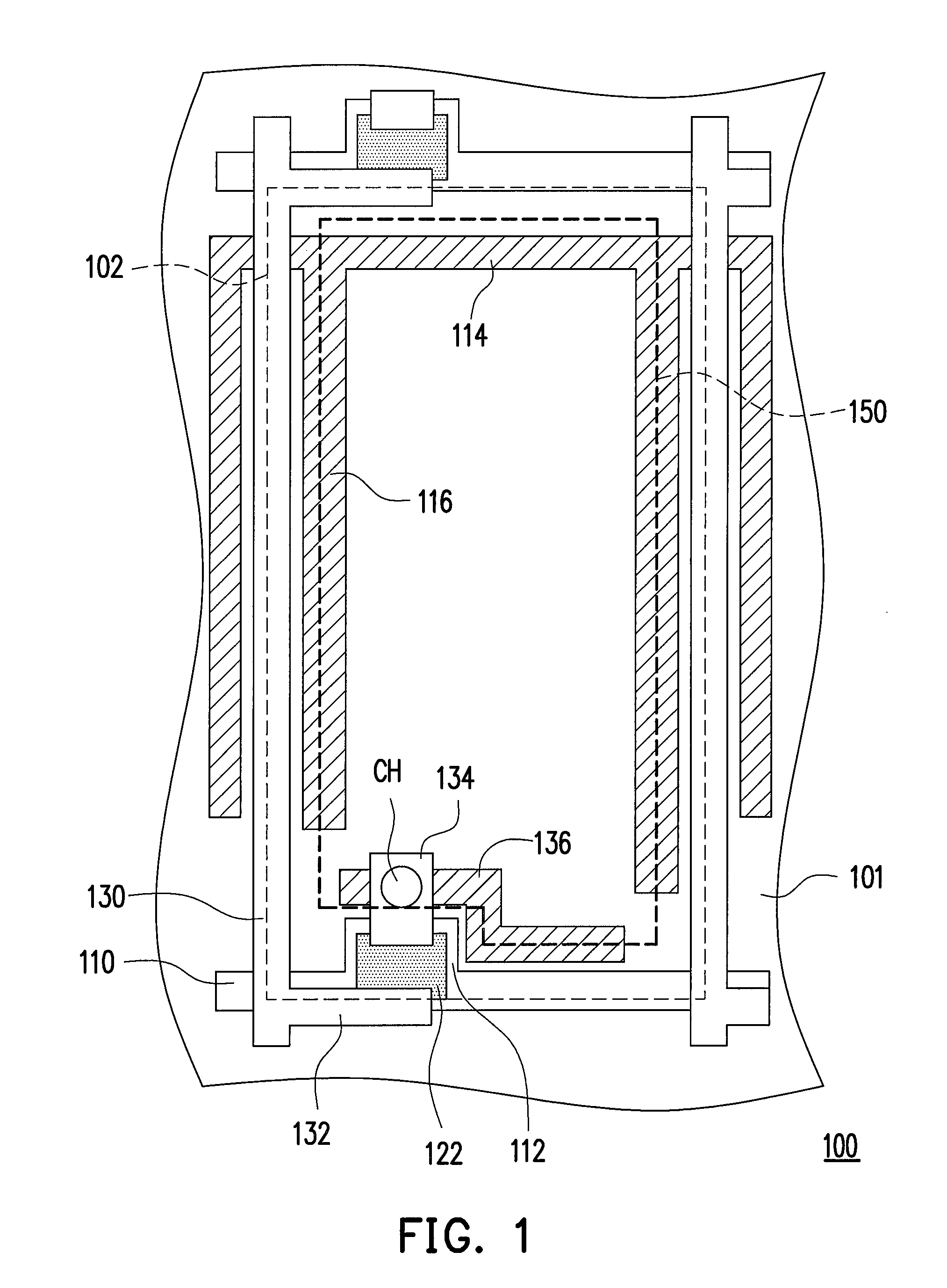
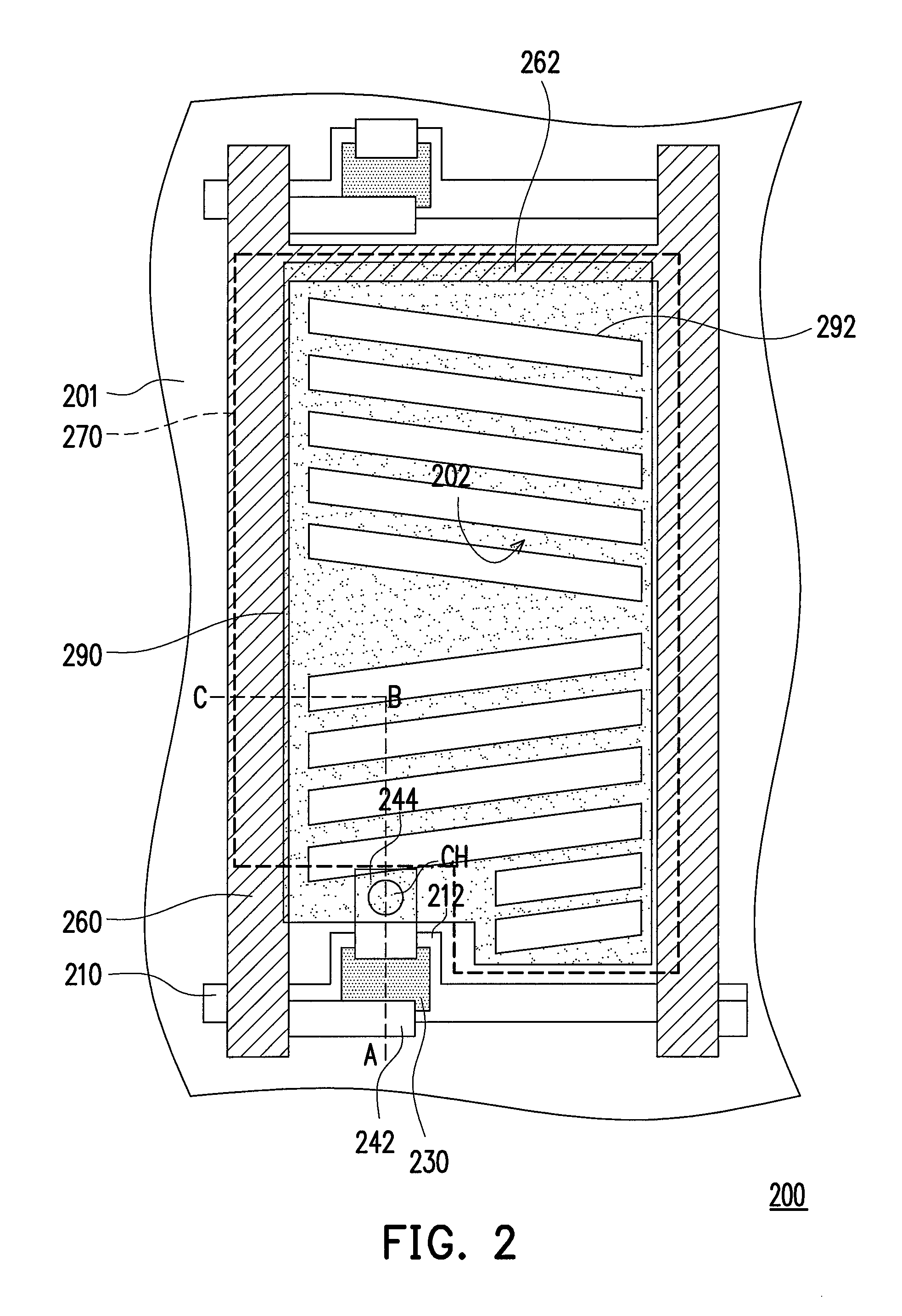
[0040]FIG. 2 is a schematic top view of a pixel structure according to an embodiment of the invention. FIGS. 3A and 3B are schematic cross-sectional views along lines A-B and B-C in FIG. 2 respectively.

[0041]Referring to all FIGS. 2, 3A, and 3B, a pixel structure 200 is disposed on a substrate 201. The substrate 201 includes a plurality of pixel areas 202 arranged in an array, and the pixel structure 200 is disposed in each of the pixel areas 202. In order to simplify the description, FIG. 2 only depicts one of the pixel areas 202. The pixel struc...


PUM


Abstract

In a fabricating method of a pixel structure, a scan line and a gate electrode are formed in each pixel area of a substrate. A gate insulation layer is formed to cover the scan line and gate electrode. A semiconductor layer is formed on the gate insulation layer above the gate electrode. A data line, source and drain are formed in each pixel area. A first passivation layer covers the data line, source and drain. A common line is formed on the first passivation layer and overlaps with at least a portion of the data line. A common electrode is formed on and electrically connected with the common line. A second passivation layer covers the common electrode and common line. A contact window is formed in the second passivation layer above the drain to expose the drain. A pixel electrode is electrically connected with the drain through the contact window.

Description

CROSS-REFERENCE TO RELATED APPLICATION[0001]This application claims the priority benefit of Taiwan application serial no. 99200888, filed Jan. 15, 2010. The entirety of the above-mentioned patent application is hereby incorporated by reference herein and made a part of specification.BACKGROUND OF THE INVENTION[0002]1. Field of Invention[0003]The invention is related to a pixel structure and a fabricating method thereof, and is particularly related to a pixel structure having a high aperture ratio and favorable display quality and a fabricating method thereof.[0004]2. Description of Related Art[0005]With advantages of high definition, small size, light weight, low driving voltage, low power consumption, and an extensive range of applications, liquid crystal displays (LCD) have replaced cathode ray tube (CRT) displays and have become the mainstream among the latest generation of display products. A conventional liquid crystal panel is formed by a color filter substrate, a thin-film tr...

Claims


Application Information

Patent Timeline
Patent Type & Authority Patents(United States)
IPC IPC(8): H01L29/04
CPCG02F1/1362H01L27/124H01L27/1259
Inventor LIOU, MENG-CHICHEN, LI-HSUAN
Owner CHUNGHWA PICTURE TUBES LTD
Why Eureka
Try Eureka