Pixel circuit, driving method thereof, electro-optical apparatus and electronic device

Inactive Publication Date: 2012-04-26
SEIKO EPSON CORP
View PDF15 Cites 3 Cited by
  • Summary
  • Abstract
  • Description
  • Claims
  • Application Information

AI Technical Summary

Benefits of technology

[0025]In addition, in the above electro-optical apparatus, it is preferred that, with respect to the pixel circuit in which a voltage according to brightness of the first light emitting element is written as the writing voltage in the writing period, in the light emitting period, the potentials of the first power line and the second power line corresponding to the respective pixel circuit are changed so that current flows from the second capacitor to the first light emitting element, and that, with respect to the pixel circuit in which a voltage according to brightness of the second light emitting element is written as the writing voltage in the writing period, in the light emitting period, the potentials of the first power line and the second power line corresponding to the respective pixel circuit are changed so that current flows from the first capacitor to the second light emitting element. According to the aspect of the invention, since the potentials of both of the first power line and the second power line

Problems solved by technology

In order to realize two-screen display without deteriorating the detail of display in comparison to a general one-screen display device, it is necessary t

Method used


Image

  • Pixel circuit, driving method thereof, electro-optical apparatus and electronic device
  • Pixel circuit, driving method thereof, electro-optical apparatus and electronic device
  • Pixel circuit, driving method thereof, electro-optical apparatus and electronic device

Examples


first embodiment

A: First Embodiment

[0047]Hereinafter, various embodiments of the invention will be described with reference to the accompanying drawings. In the drawings, the dimensions and ratios of each component are suitably changed from actual ones.

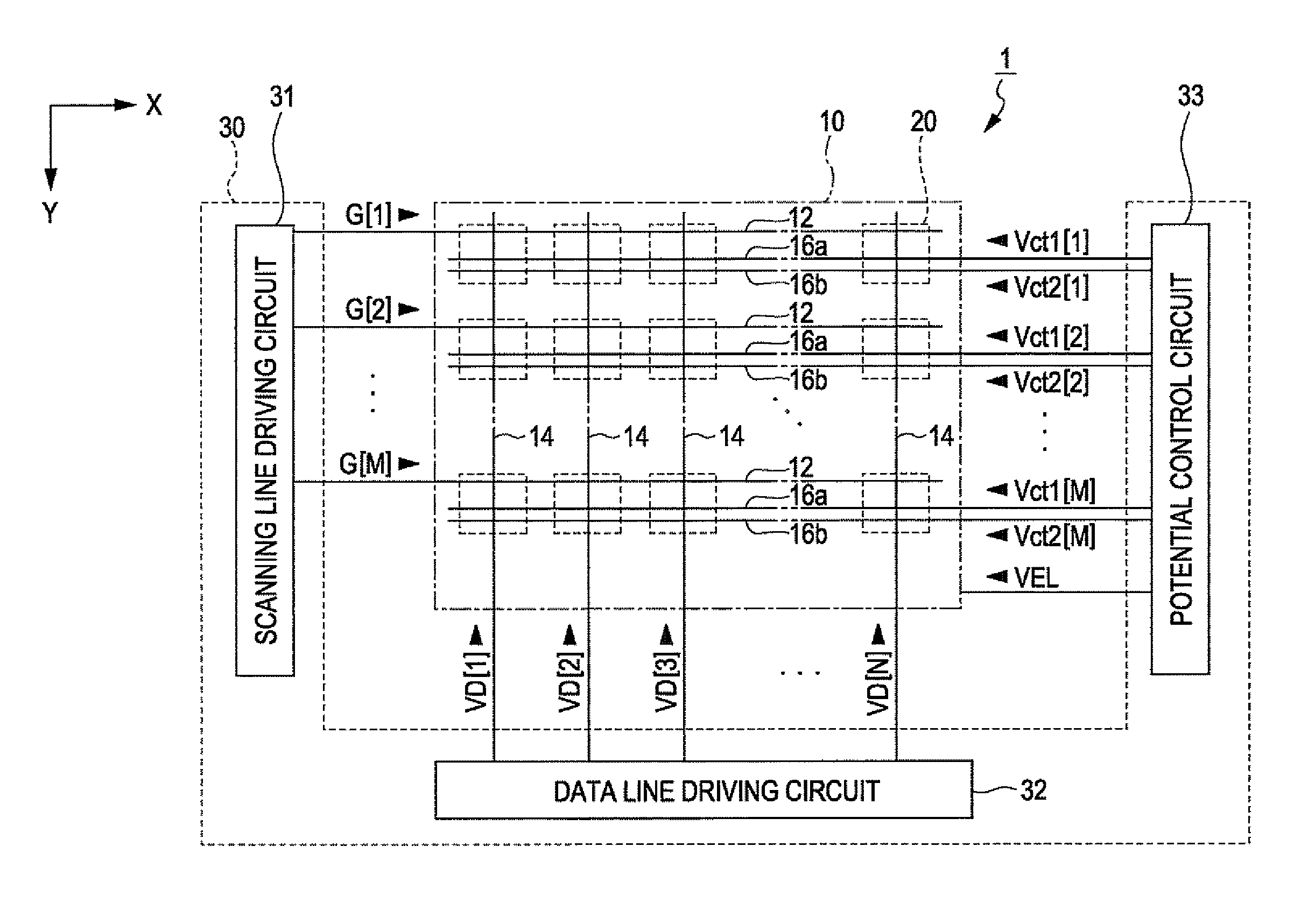
[0048]FIG. 1 is a block diagram showing a display device 1 according to the first embodiment of the invention. The display device 1 includes a display region 10 in which a plurality of pixel circuits 20 are arranged, and a driving circuit 30 for driving each pixel circuit 20. The driving circuits 30 are distributed and mounted to, for example, a plurality of integrated circuits. However, at least a part of the driving circuits 30 may be configured as a thin film transistor formed on a substrate together with the pixel circuit 20.

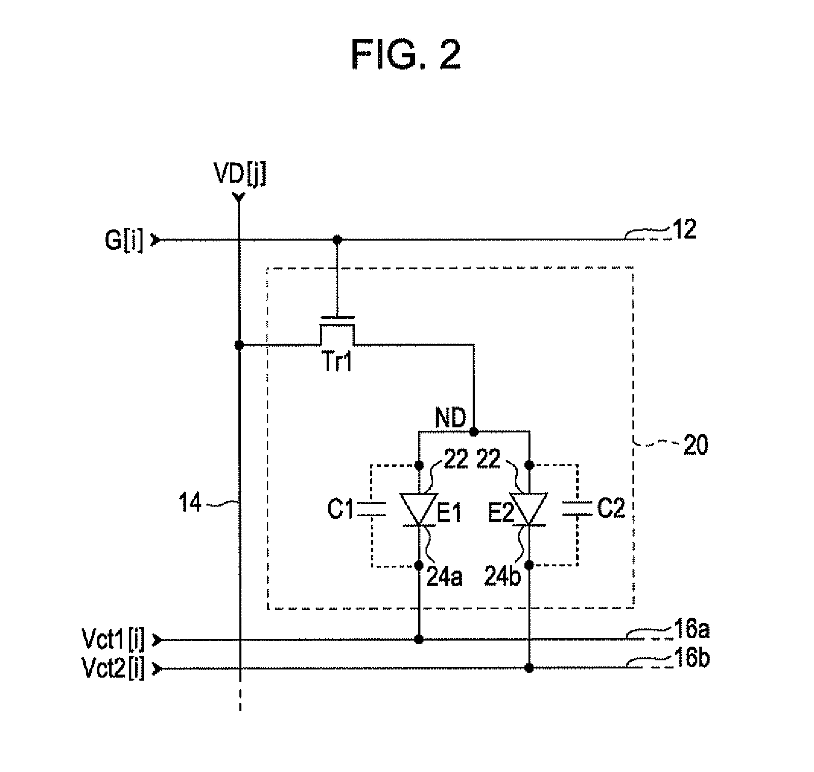
[0049]In the display region 10, M number of scanning lines 12 extending in an X direction, M number of first power lines 16a and M number of second power lines 16b extending in the X direction, and N number of data lines 14 e...

second embodiment

B: Second Embodiment

[0110]The display device according to the first embodiment is configured so that the first power potential Vct1[i] is the fixed potential Vcst and the second power potential Vct2[i] has a lamp waveform, whereby the first light emitting element E1 emits light and the second light emitting element E2 does not emit light. In contrast to this, the display device according to the second embodiment is different from the display device of the first embodiment in the points that the first power potential Vct1[i] is any one of the fixed potential Vcst and the lamp waveform and the second power potential Vct2[i] is the other, and that the one and the other take turns at every one vertical scanning period.

[0111]The display device of the second embodiment is configured identically to the display device 1 of the first embodiment, except that the first power potential Vct1[i] and the second power potential Vct2[i] generated by the potential control circuit 33 have different wa...

third embodiment

C: Third Embodiment

[0124]FIG. 12 is a timing chart for illustrating operations of a display device according to a third embodiment.

[0125]The display device of the third embodiment is configured identical to the display device 1 of the first embodiment, except that the first power potential Vct1[i] and the second power potential Vct2[i] generated by the potential control circuit 33 have different waveforms.

[0126]In other words, in the first embodiment, the second power potential Vct2[i] has a lamp waveform varying between the first potential VL and the second potential VH, and the first power potential Vct1[i] is maintained at the fixed potential Vcst. In this regard, in the third embodiment, the first power potential Vct1[i] and the second power potential Vct2[i] are output from the potential control circuit 33 so as to have a waveform periodically varying between the first potential VL and the second potential VH.

[0127]As shown in FIG. 12, in the period when the selection signal G[...


PUM


Abstract

A pixel circuit includes a first light emitting element having a first opposite electrode connected to a first power line, a common electrode and a parasitic capacitance C1; and a second light emitting element having a second opposite electrode connected to a second power line, a common electrode and a parasitic capacitance C2. A first power potential is supplied to the first power line, and a second power potential is supplied to the second power line. The first and second power potentials change by increasing with a constant gradient from a low first potential to a high second potential in turns, and the first and second light emitting elements emit light in turns by flowing current from the parasitic capacitance C1 or C2 to the other light emitting element.

Description

BACKGROUND[0001]1. Technical Field[0002]The present invention relates to a pixel circuit having a light emitting element such as an organic EL (Electroluminescence) element, a driving method thereof, an electro-optical apparatus, and an electronic device.[0003]2. Related Art[0004]Recently, demand for two-screen display devices displaying two different images in right and left portions and 3D display devices outputting a right eye image and a left eye image together for 3D displaying has increased along with the propagation of car navigation systems, 3D TVs with a two-screen displaying function, and the like.[0005]Generally, a two-screen display device arranges pixels for displaying a right image and pixels for displaying a left image in turns to optically divide right and left images by an optic device corresponding to pixels such as a lenticular lens or a parallax barrier between pixels and an observer so that different images are displayed in the right and left portions.[0006]In a...

Claims


Application Information

Patent Timeline
IPC IPC(8): G09G5/10H05B37/02
CPCG09G3/20G09G3/003H01L51/50G09G3/30G09G3/2014G09G3/2074G09G3/3258G09G2300/0443G09G2300/0804G09G2310/0259G09G2310/066
Inventor KUBOTA, TAKEHIKO
Owner SEIKO EPSON CORP
Why Eureka
Try Eureka