Methods and apparatus for controlling photoresist line width roughness

a technology of photoresist and line width, applied in the direction of electrical equipment, decorative arts, electric discharge tubes, etc., can solve the problems of difficult to control the rough edges of the photoresist layer, the difficulty of lithography process to transfer even smaller features precisely and accurately onto the substrate, and the evolution of the integrated circuit into complex devices

Active Publication Date: 2012-05-03
APPLIED MATERIALS INC
View PDF5 Cites 371 Cited by
  • Summary
  • Abstract
  • Description
  • Claims
  • Application Information

AI Technical Summary

Benefits of technology

[0011]In yet another embodiment, a method for controlling line width roughness of a photoresist layer disposed on a substrate includes supplying a gas mixture into a processing chamber having a substrate disposed therein, wherein the substrate has a patterned photoresist layer disposed thereon, applying a microwave power to the processing chamber to generate an electric field in the p

Problems solved by technology

Integrated circuits have evolved into complex devices that can include millions of components (e.g., transistors, capacitors and resistors) on a single chip.
Accordingly, lithography process has become more and more challenging to transfer even smaller features onto a substrate precisely and accurately without damage.
However, at such small dimensions, the roughness of the edges of a photoresist layer has become harder and

Method used


Image

  • Methods and apparatus for controlling photoresist line width roughness
  • Methods and apparatus for controlling photoresist line width roughness
  • Methods and apparatus for controlling photoresist line width roughness

Examples


Embodiment Construction

[0021]Embodiments of the present invention include methods and apparatus for controlling line width roughness (LWR) of a photoresist layer disposed on a substrate. The line width roughness (LWR) of a photoresist layer may be controlled by performing an electron cyclotron resonance (ECR) plasma process on a photoresist layer after an exposure / development process. The electron cyclotron resonance (ECR) plasma process is performed to provide a chemical and electron grinding process in a nanometer scale to smooth the edge of the photoresist layer pattern, thereby providing a smooth pattern edge of the photoresist layer with minimum pattern edge roughness for the subsequent etching process.

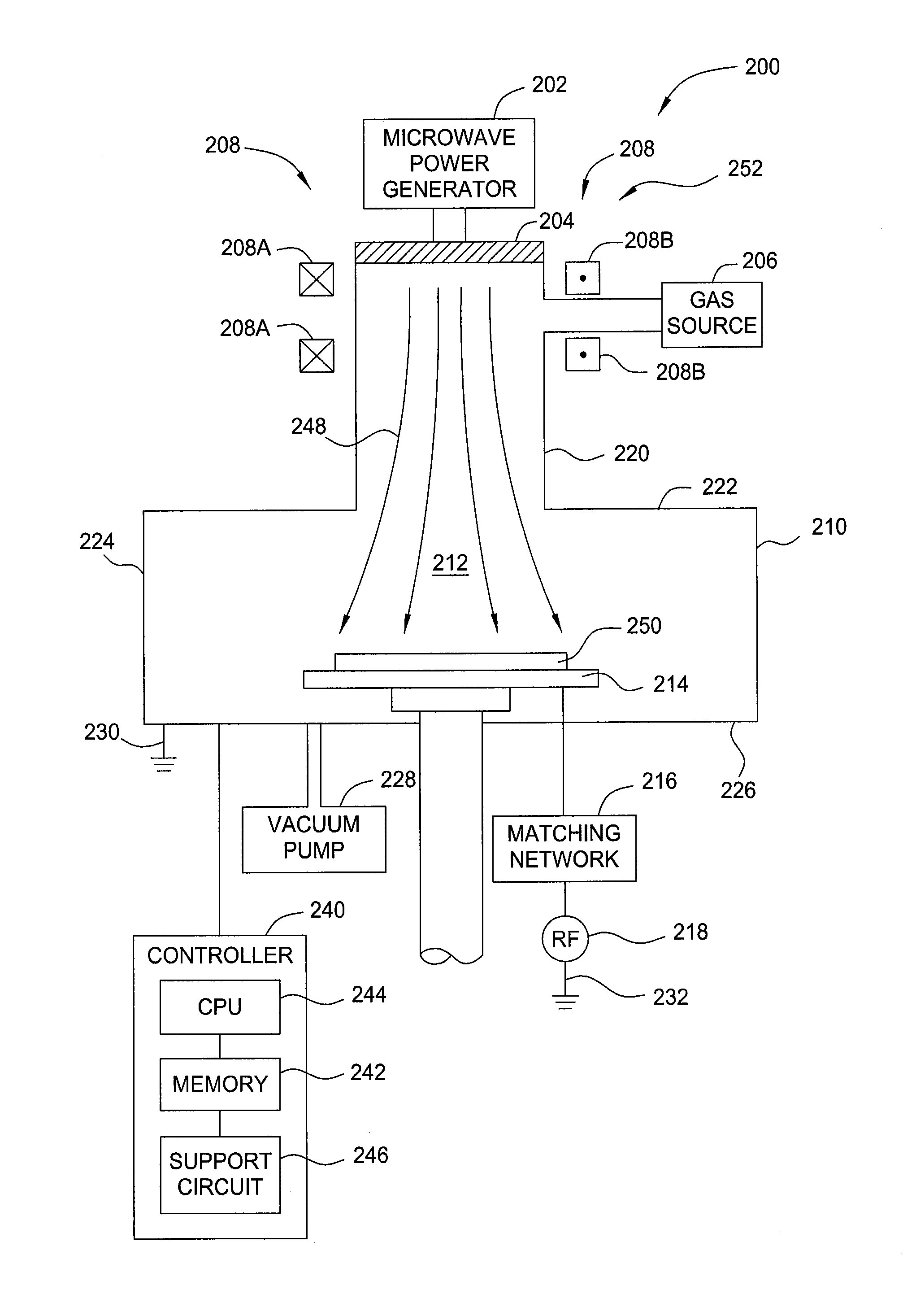
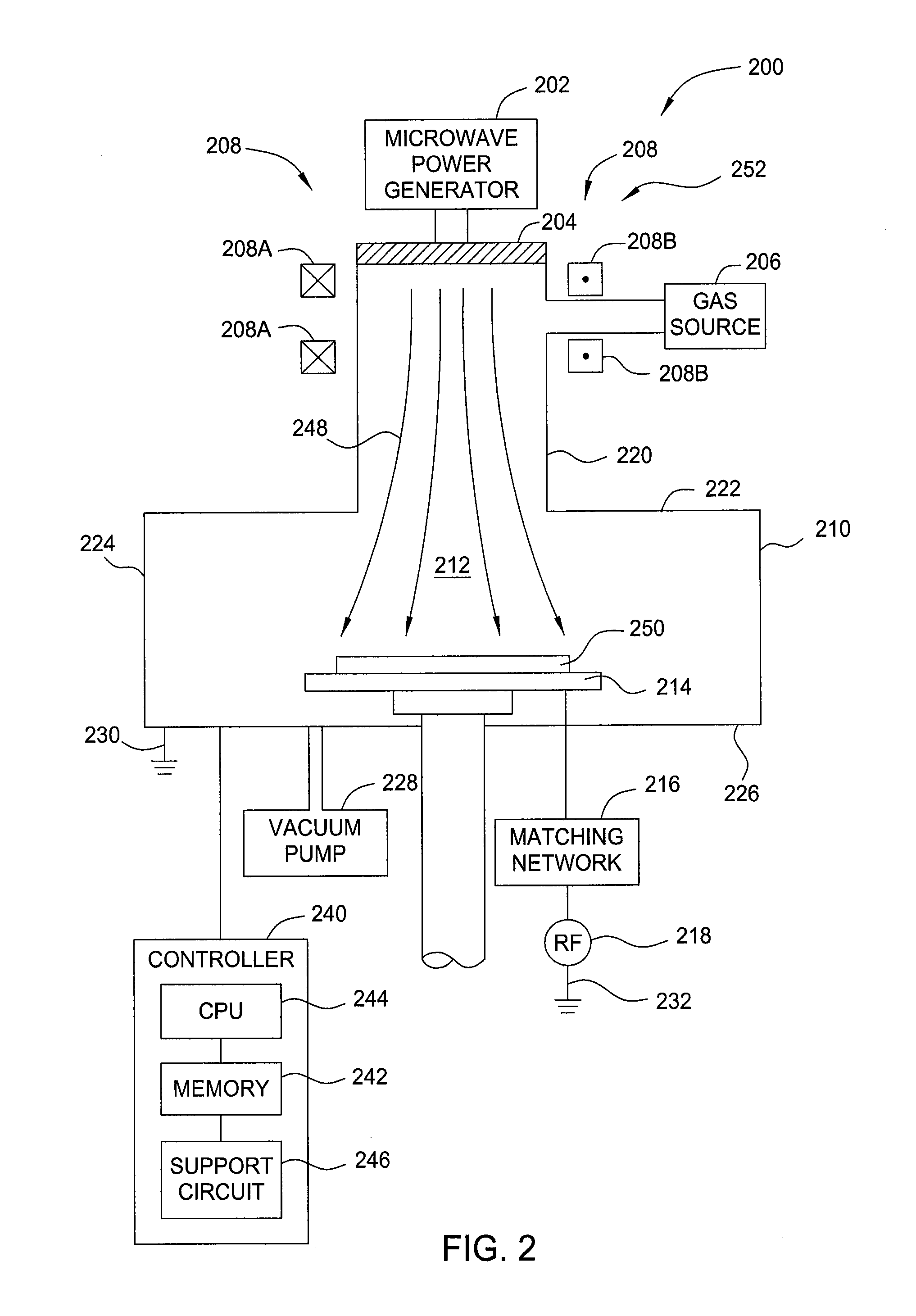
[0022]FIG. 2 depicts a schematic, cross-sectional diagram of one embodiment of a electron cyclotron resonance (ECR) plasma reactor 200 suitable for performing an electron cyclotron resonance (ECR) plasma process according to the present invention. One such etch reactor suitable for performing the inven...


PUM

PropertyMeasurementUnit
Widthaaaaaaaaaa
Surface roughnessaaaaaaaaaa
Poweraaaaaaaaaa

Abstract

The present invention provides methods and an apparatus for controlling and modifying line width roughness (LWR) of a photoresist layer. In one embodiment, an apparatus for controlling a line width roughness of a photoresist layer disposed on a substrate includes a chamber body having a top wall, side wall and a bottom wall defining an interior processing region, a microwave power generator coupled to the to the chamber body through a waveguild, and one or more coils or magnets disposed around an outer circumference of the chamber body adjacent to the waveguide, and a gas source coupled to the waveguide through a gas delivery passageway.

Description

CROSS-REFERENCE TO RELATED APPLICATIONS[0001]This application claims benefit of U.S. Provisional Application Ser. No. 61 / 407,209 filed Oct. 27, 2010 (Attorney Docket No. APPM / 15447L), which is incorporated by reference in their entirety.BACKGROUND[0002]1. Field of the Invention[0003]The present invention generally relates to methods and apparatus for controlling photoresist line width roughness and, more specifically, to methods and apparatus for controlling photoresist line width roughness in semiconductor processing technologies.[0004]2. Description of the Related Art[0005]Integrated circuits have evolved into complex devices that can include millions of components (e.g., transistors, capacitors and resistors) on a single chip. The evolution of chip designs continually requires faster circuitry and greater circuit density. The demands for greater circuit density necessitate a reduction in the dimensions of the integrated circuit components.[0006]As the dimensions of the integrated...

Claims


Application Information

Patent Timeline
IPC IPC(8): C23F1/00C23F1/08
CPCH01J37/32192H01J37/3266H01L21/31138H01J2237/3343H01L21/0273H01J37/32678
Inventor WU, BANQIUKUMAR, AJAY
Owner APPLIED MATERIALS INC
Why Eureka
Try Eureka