White ceramic LED package

a technology of led packaging and white ceramics, applied in the field of white, thin/low-profile packaging, can solve the problems of affecting so as to improve the quality of led packaging, improve the color mixing and emission, and improve the structural integrity

Active Publication Date: 2012-05-03
CREELED INC
View PDF7 Cites 64 Cited by
  • Summary
  • Abstract
  • Description
  • Claims
  • Application Information

AI Technical Summary

Benefits of technology

[0011]The present invention provides leadless emitter packages for LED displays and the like that provide for improved color mixing and emission, with the emitter packages being thin / low profile for flatter applications and / or small for small panel applications. The present invention also provides emitter packages with improved structural integrity, with the packages having suitable surface area for mounting a desired number of LED chips and corresponding components.
[0013]Pursuant to another embodiment, a ceramic emitter package is provided comprising a white casing with a cavity extending into the interior of the casing from a top surface of the casing and electrically conductive bond pads integral to the casing, with a first set of the bond pads comprising chip carrier parts, and a second set of the bond pads comprising connection parts. A plurality of light emitting devices are arranged on the first set of bond pads, with the light emitting devices and portions of the bond pads exposed through the cavity. A plurality of electrodes are also provided, which are disposed at least on the bottom surface of the casing. U-shaped indentations are also provided in one or more of the side surface of the casing. One or more of the bond pads comprises features to improve the connection between the bond pads and the casing.

Problems solved by technology

Moreover, each individual LED in a module and its respective emissions should not be readily and individually visible when a pixel module is illuminated via light emitting from one or more of its LEDs.
The thin / low profile packages and / or small packages are expected to maintain their structural integrity during manufacture and use, but the integrity of such packages can become compromised.
For example, the package structures can become deformed during the reflow process or damaged during the cutting process.
Furthermore, packages may experience separation between the package casing and the bonding pads during manufacture and use.

Method used


Image

  • White ceramic LED package
  • White ceramic LED package
  • White ceramic LED package

Examples


Embodiment Construction

[0029]The present invention is described herein with reference to certain embodiments, but it is understood that the invention can be embodied in many different forms and should not be construed as limited to the embodiments set forth herein.

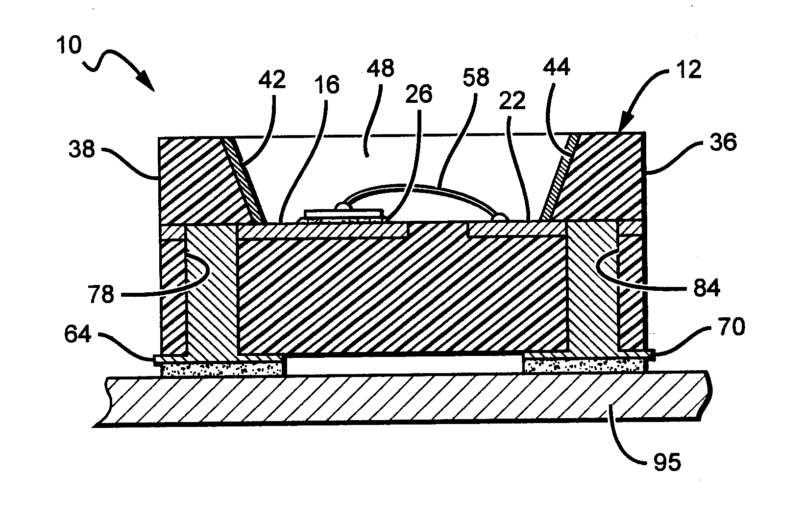
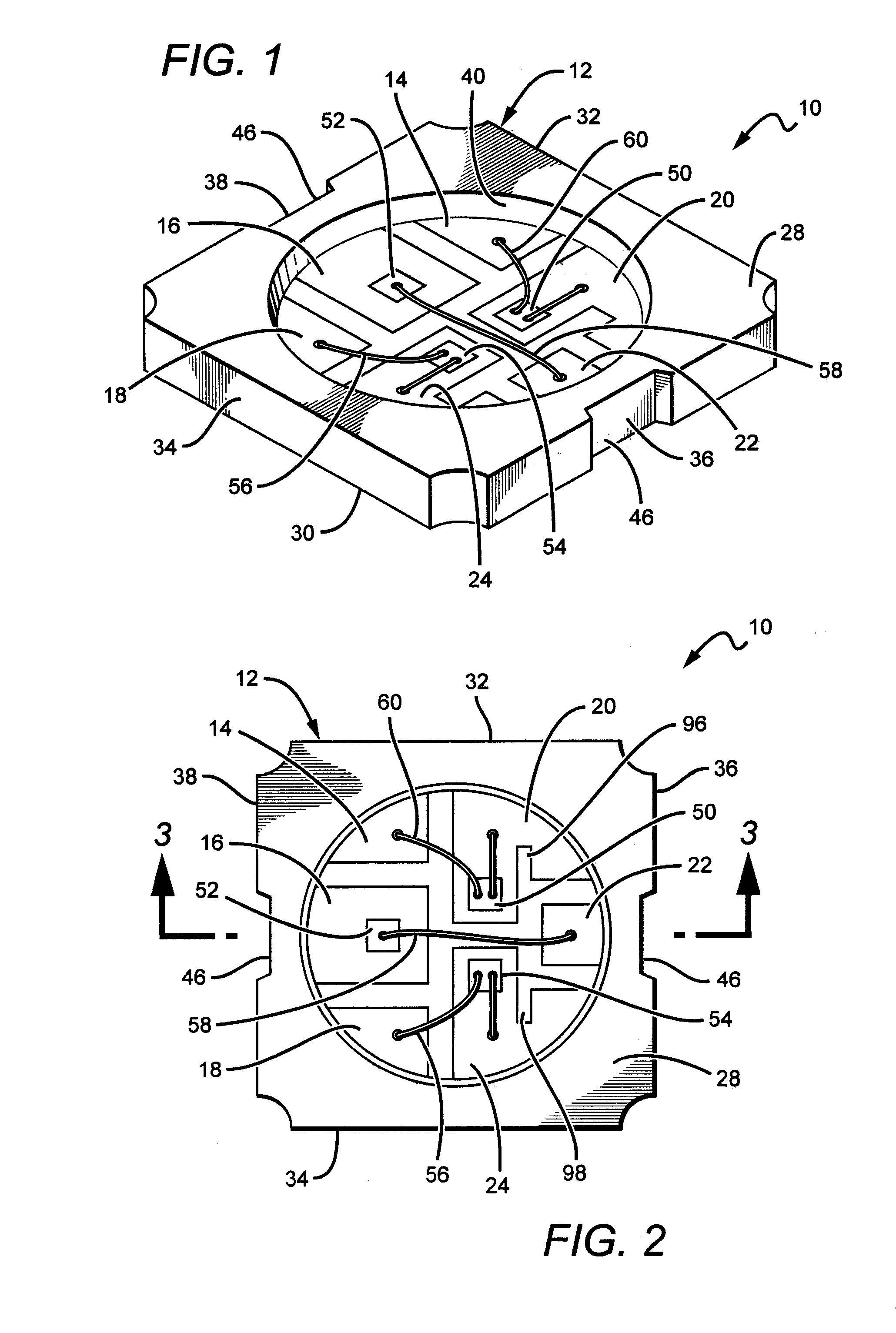
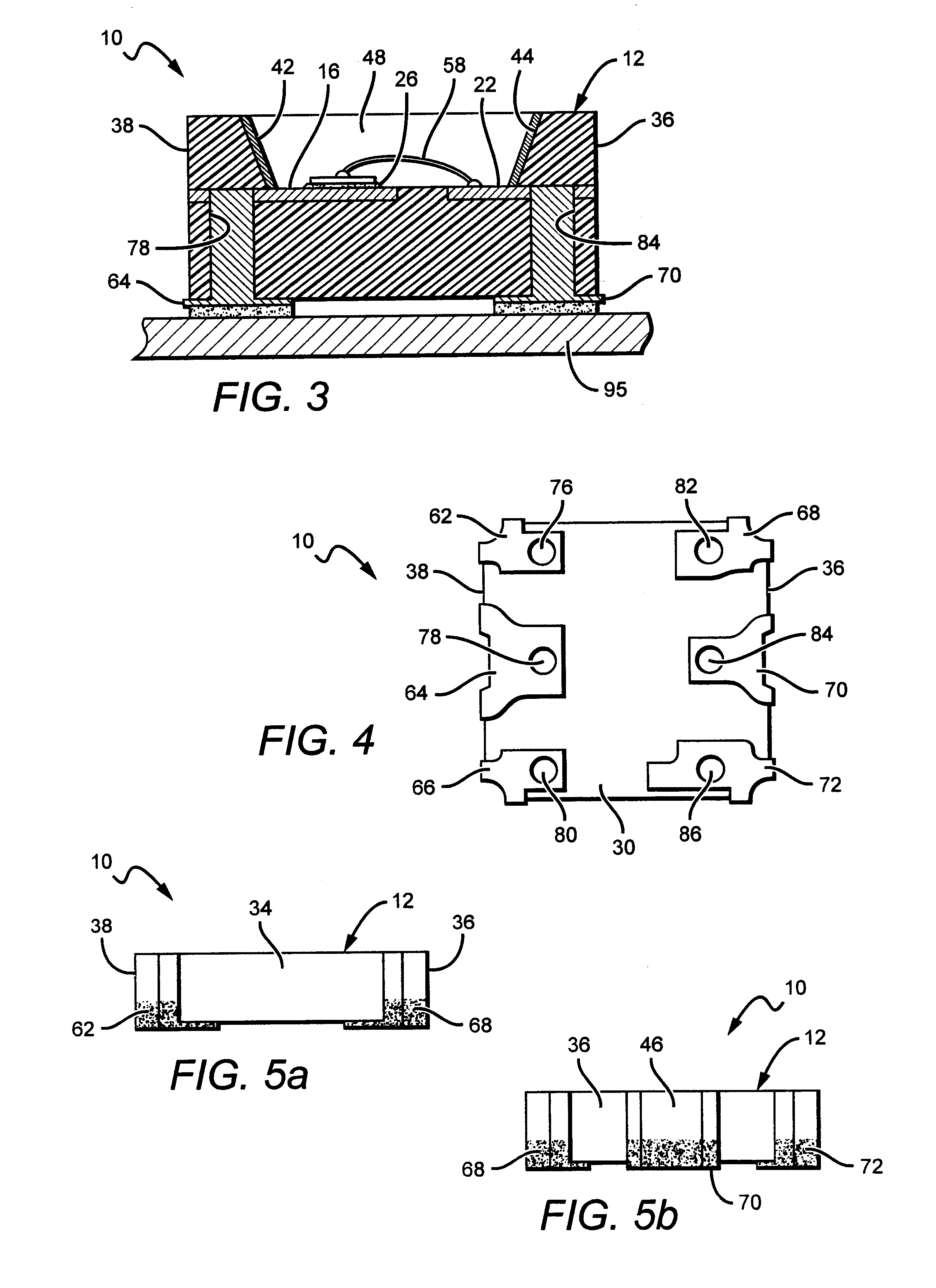
[0030]In some embodiments according to the present invention, structures are provided for multiple emitter packages that allow the packages to emit light with improved color mixing by providing reflective white ceramics packages and non-linearly placing the emitters within the package. Moreover, some embodiments of the present invention provide leadless packages, which can help reduce the overall depth of the package while still maintaining electrical connection between electrodes and light emitting devices via through-holes. As such, the leadless configuration may result in overall packages that are much thinner for use in lower profile applications.

[0031]Moreover, some embodiments of the present invention provide emitter packages that maintain...


PUM

PropertyMeasurementUnit
heightaaaaaaaaaa
heightaaaaaaaaaa
heightaaaaaaaaaa

Abstract

The present invention is directed to leadless LED packages and LED displays utilizing white ceramic casings and thin / low profile packages with improved color mixing and structural integrity. In some embodiments, the improved color mixing is provided, in part, by the white ceramic package casing, which can help reflect light emitted from each LED in many directions away from the device. The non-linear arrangement of the LEDs can also contribute to improved color-mixing. The improved structural integrity can be provided by various features in the bond pads that cooperate with the casing for a stronger package structure. Moreover, in some embodiments the thinness / low profile of each package is attributed to its leadless structure, with the bond pads and electrodes electrically connected via through-holes. In some embodiments, the structural integrity of the package can also be attributed to indentations along its sides, which do not enable as much plating material to accumulate at the sides and helps package cutting processes during manufacture. The indentations can also contribute to displays having more tightly and densely packed LED arrays.

Description

BACKGROUND OF THE INVENTION[0001]1. Field of the Invention[0002]The present invention relates generally to electronic packaging, and more particularly to white, thin / low profile packaging having multiple emitters.[0003]2. Description of the Related Art[0004]Light emitting diodes (LEDs) are solid state devices that convert electric energy to light, and generally comprise one or more active layers of semiconductor material sandwiched between oppositely doped layers. When a bias is applied across the doped layers, holes and electrons are injected into the active layer where they recombine to generate light. Light is emitted from the active layer and from all surfaces of the LED.[0005]In recent years, there have been dramatic improvements in LED technology such that LEDs with increased brightness and color fidelity, smaller footprints, and overall improved emitting efficiency have been introduced. LEDs also have an increased operation lifetime compared to other emitters. For example, th...

Claims


Application Information

Patent Timeline
Patent Type & Authority Applications(United States)
IPC IPC(8): H01L33/08H01L33/50H01L33/38
CPCH01L25/0753H01L33/486H01L33/62H01L2924/09701H01L2224/73265H01L2224/48091H01L2924/00014H01L2924/00
Inventor CHAN, ALEX CHI KEUNGPANG, CHARLES CHAK HAULAU, VICTOR YUE KWONG
Owner CREELED INC
Why Eureka
Try Eureka