Eureka AIR delivers breakthrough ideas for toughest innovation challenges, trusted by R&D personnel around the world.

Metal silicide formation

a technology of metal silicide and contact pads, which is applied in the field of new metal silicide contact pads and processes, can solve the problems of junction leakage, line width limitations, and the end of the trend of ever smaller and denser devices

Active Publication Date: 2012-05-03
MACRONIX INT CO LTD
View PDF3 Cites 6 Cited by
  • Summary
  • Abstract
  • Description
  • Claims
  • Application Information

AI Technical Summary

Benefits of technology

[0010]Disclosed herein are novel processes for forming metal silicide contact pads on semiconductor devices. For example, in some embodiments, disclosed are techniques for forming cobalt silicide contact pads on and between wordlines formed on a semiconductor device. Of course, other metal silicides may be formed on and between other types of raised silicon-based features using the disclosed techniques.
[0011]In one exemplary embodiment, a method for forming metal silicide contact pads on semiconductor devices may comprise depositing a metal layer on and between a plurality of raised silicon-based features formed on a semiconductor substrate, the metal layer comprising metal capable of reacting with external silicon-based portions of the features to form a metal silicide. In addition, such a method may also include depositing a cap layer on the metal layer deposited on and between the plurality of raised silicon-based features, wherein a thickness of the cap layer on the metal layer between the raised features is greater than or equal to a thickness of the cap layer on the metal layer on the raised features. Furthermore, such a method may also include annealing the structure to cause portions of the metal layer to react with portions of the external silicon-based portions of the features to form metal silicide pads on and between the raised features.
[0012]In another embodiment, a method of forming metal silicide contact pads on a semiconductor device may comprise depositing a first metal layer on and between a plurality of raised silicon-based features, wherein a thickness of the first metal layer on the raised features is greater than a thickness of the first metal layer between the raised features, and wherein the first metal layer comprises metal capable of reacting with external silicon-based portions of the features to form a metal silicide. Additionally, in this embodiment of the method, the method may further comprise depositing a second metal layer on the first metal layer deposited on and between the plurality of raised silicon-based features, wherein the first and s

Problems solved by technology

Thus, semiconductor device improvements have been largely accomplished by reducing device feature size to the point where currently micron and sub-micron device features are being used, and predictions for future device sizes do not foresee an end to the trend of ever smaller and denser devices.
In view of the above, while salicide formed on gates and source / drain regions reduces parasitic resistance, line width limitations challenge salicide implementation in smaller features and devices.
However, cobalt and cobalt salicide (CoSiX), for example, in transistor applications, can penetrate into the junction area, resulting in junction leakage, increase in contact resistance, and deteriorating transistor current drive.
Generally speaking, high temperatures are required for reacting cobalt and silicon, and a significant portion of the silicon substrate gets consumed in the process, causing the undesirable changes in the gate junction depth.
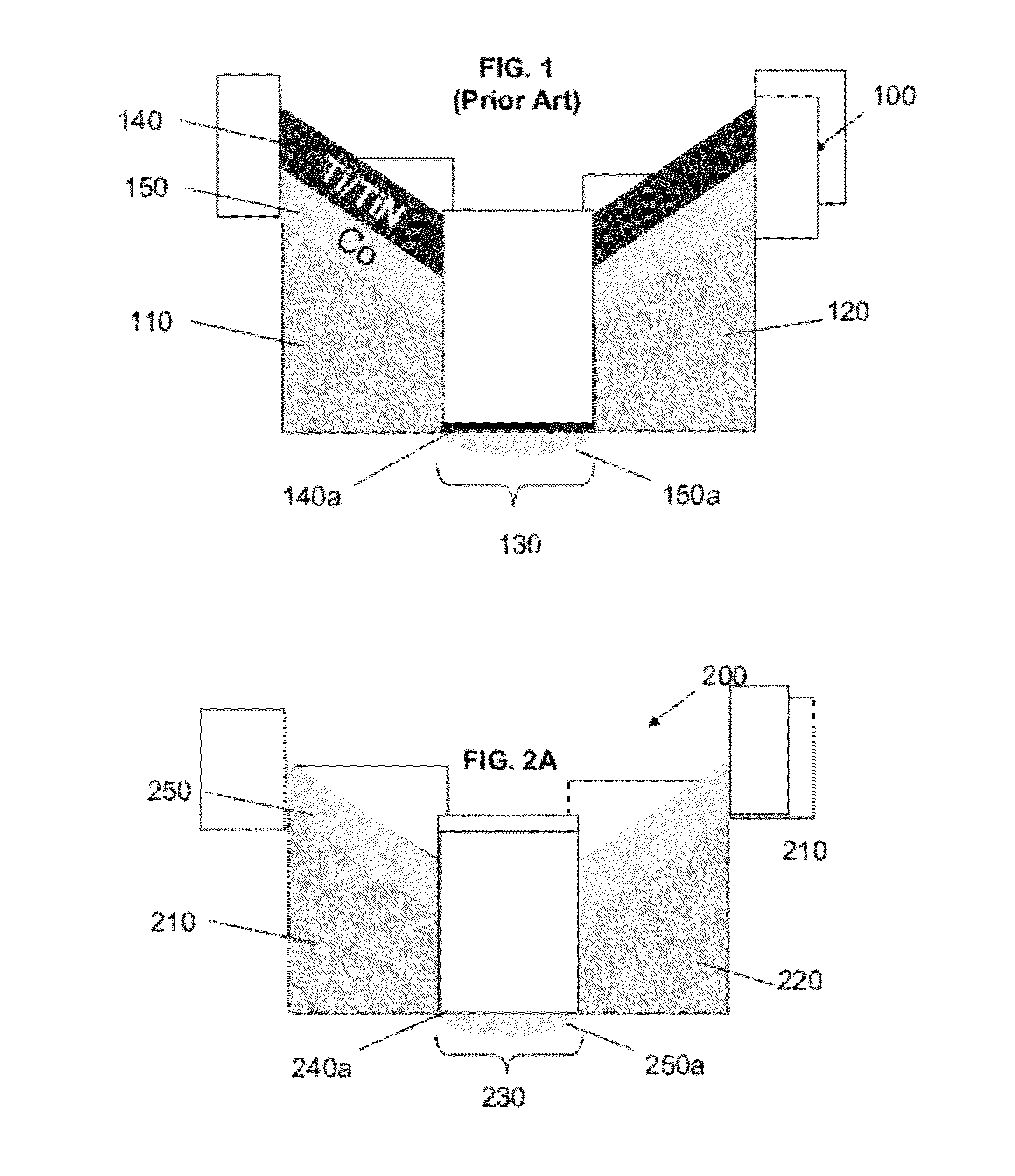
However, the conventional process for depositing a Ti / TiN cap over the cobalt typically results in poor step coverage.
However, in conventional processes, the Ti / TiN cap 140a deposition results in poor step coverage.
Additionally, the insufficient thickness of the Ti / TiN cap 140a over the source / drain region 130 increases the possibility of agglomeration of the cobalt during the silicide process, which often results in leakage of the finished device.

Method used


Image

  • Metal silicide formation
  • Metal silicide formation
  • Metal silicide formation

Examples


Embodiment Construction

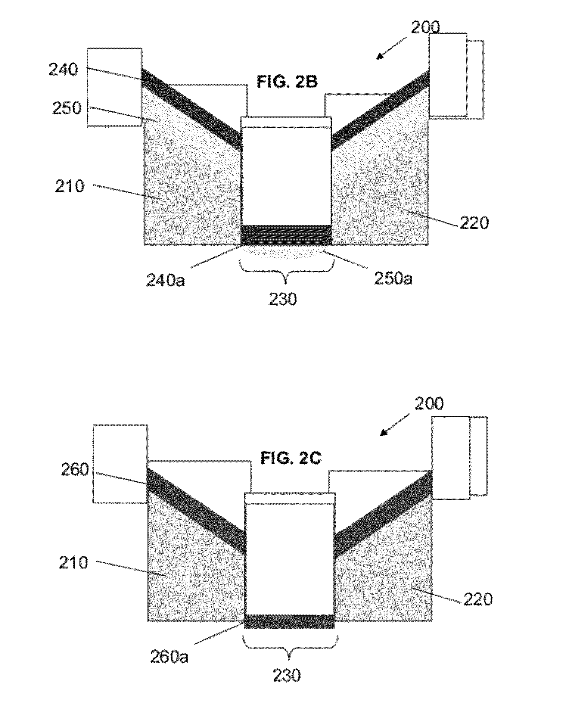
[0018]FIG. 2A illustrates a cross-sectional view of a semiconductor device 200 in the process of being fabricated in accordance with one embodiment of the disclosed principles. As shown in FIG. 2A, the semiconductor device 200 includes raised device features 210, 220, which in an exemplary embodiment are wordlines 210, 220 formed on a substrate. In such exemplary embodiments, the wordlines 210, 220 may be formed to a thickness of about 300˜5 kÅ. Of course, the raised features 210, 220 may also be other device features on which a metal silicide, or a salicide, contact pad will be formed. Typically, the raised features 210, 220 comprise polysilicon, but they may also comprise other silicon-based materials that can be reacted with metals to form metal silicide on the exterior surface thereof.

[0019]Also illustrated in FIG. 2A, in accordance with the disclosed principles, a metal layer 250 is deposited directly on the wordlines 210, 220, as well as a metal layer 250a being deposited dire...


PUM


Abstract

Techniques for forming metal silicide contact pads on semiconductor devices are disclosed, and in one exemplary embodiment, a method may comprise depositing a metal layer on and between a plurality of raised silicon-based features formed on a semiconductor substrate, the metal layer comprising metal capable of reacting with external silicon-based portions of the features to form a metal silicide. In addition, such a method may also include depositing a cap layer on the metal layer deposited on and between the plurality of raised silicon-based features, wherein a thickness of the cap layer on the metal layer between the raised features is greater than or equal to a thickness of the cap layer on the metal layer on the raised features. Furthermore, such a method may also include annealing the structure to cause portions of the metal layer to react with portions of the external silicon-based portions of the features to form metal silicide pads on and between the raised features.

Description

BACKGROUND[0001]1. Technical Field[0002]The present disclosure relates in general to the manufacture of semiconductor devices, and more particularly to novel processes for forming metal silicide contact pads on semiconductor devices.[0003]2. Related Art[0004]As technology in products and equipment continues to become more complex, the use of integrated circuit (IC) devices in these products and equipment is basically essential. In addition, consumers and manufacturers alike have continued to desire smaller product size, which requires a continued decrease in overall IC chip size. As a result, the large-scale integration of circuit components, such as transistors and capacitors, has become a necessity for decreased overall size, but increased device performance. Thus, semiconductor device improvements have been largely accomplished by reducing device feature size to the point where currently micron and sub-micron device features are being used, and predictions for future device sizes...

Claims


Application Information

Patent Timeline
IPC IPC(8): H01L29/78H01L21/28
CPCH01L21/28052H01L29/66507H01L21/28518
Inventor LUOH, TUUNGHSIEH, SHENG HUIHUANG, RICKYSU, CHIN-TAYANG, TAHONECHEN, KUANG-CHAO
Owner MACRONIX INT CO LTD
Why Eureka
Eureka Blog
Learn More