Epitaxial growth of silicon carbide on sapphire
a silicon carbide and sapphire technology, applied in the growth process of polycrystalline materials, crystal growth processes, chemically reactive gases, etc., can solve the problems of hexagonal symmetry, inability to provide a 200 mm substrate or a 300 mm substrate containing a silicon carbide layer, etc., to achieve excellent in-plane electrical conductivity and carrier mobility
- Summary
- Abstract
- Description
- Claims
- Application Information
AI Technical Summary
Benefits of technology
Problems solved by technology
Method used
Image

Examples
first embodiment
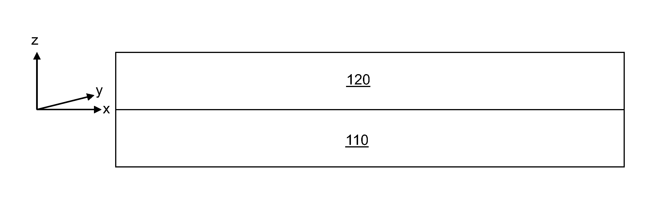
[0028]Referring to FIG. 2, a first exemplary structure including according to the present invention includes a vertical stack of a single crystalline semiconductor-carbon alloy layer 120 and a sapphire substrate 110. The single crystalline semiconductor-carbon alloy layer 120 has a hexagonal crystal structure and a (0001) surface orientation. The single crystalline semiconductor-carbon alloy layer 120 is epitaxially deposited on a (0001) surface of the sapphire substrate 110.
[0029]It is noted that, by reducing the deposition temperature or by otherwise providing inferior growth conditions, for example, by providing an ambient including a significant level of residual gases within a deposition chamber, the single crystalline semiconductor-carbon alloy layer 120 can be replaced with a polycrystalline semiconductor-carbon alloy layer including at least one polycrystalline semiconductor-carbon alloy portions each having a hexagonal crystal structure and a (0001) surface orientation and ...
second embodiment
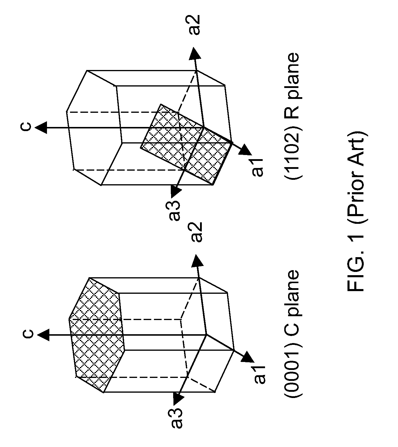
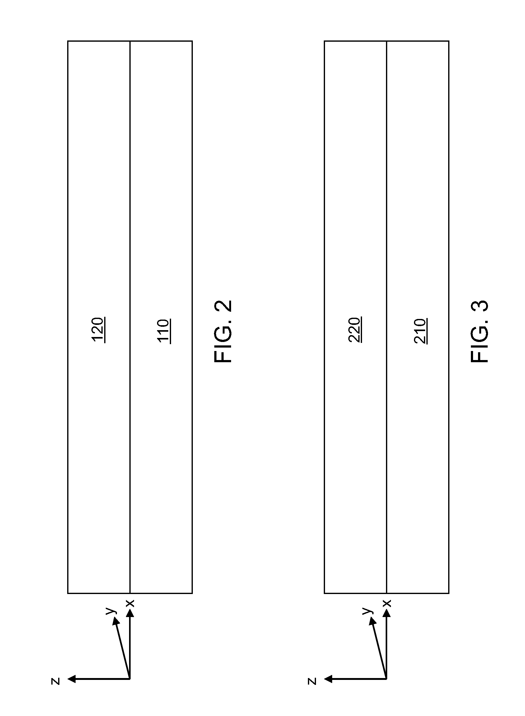
[0038]Referring to FIG. 3, a second exemplary structure including according to the present invention includes a vertical stack of a single crystalline semiconductor-carbon alloy layer 220 and a sapphire substrate 210. The single crystalline semiconductor-carbon alloy layer 220 has a cubic crystal structure of zinc blende type and a (110) surface orientation. The single crystalline semiconductor-carbon alloy layer 220 is epitaxially deposited on a (1102) surface of the sapphire substrate 210.
[0039]The sapphire substrate 210 consists essentially of aluminum oxide as in the first embodiment. The entirety of the sapphire substrate 210 is single crystalline. However, the surface orientation of the sapphire substrate 210 is a (1102) orientation. The plane of the (1102) orientation is also referred to as an R plane.
[0040]The single crystalline semiconductor-carbon alloy layer 220 is a single crystalline layer in which all atoms are epitaxially aligned to all other atoms of the single cryst...
PUM
| Property | Measurement | Unit |
|---|---|---|
| temperature | aaaaa | aaaaa |
| diameter | aaaaa | aaaaa |
| diameter | aaaaa | aaaaa |
Abstract
Description
Claims
Application Information