Method of manufacturing light emitting device
- Summary
- Abstract
- Description
- Claims
- Application Information
AI Technical Summary
Problems solved by technology
Method used
Image

Examples
example 1
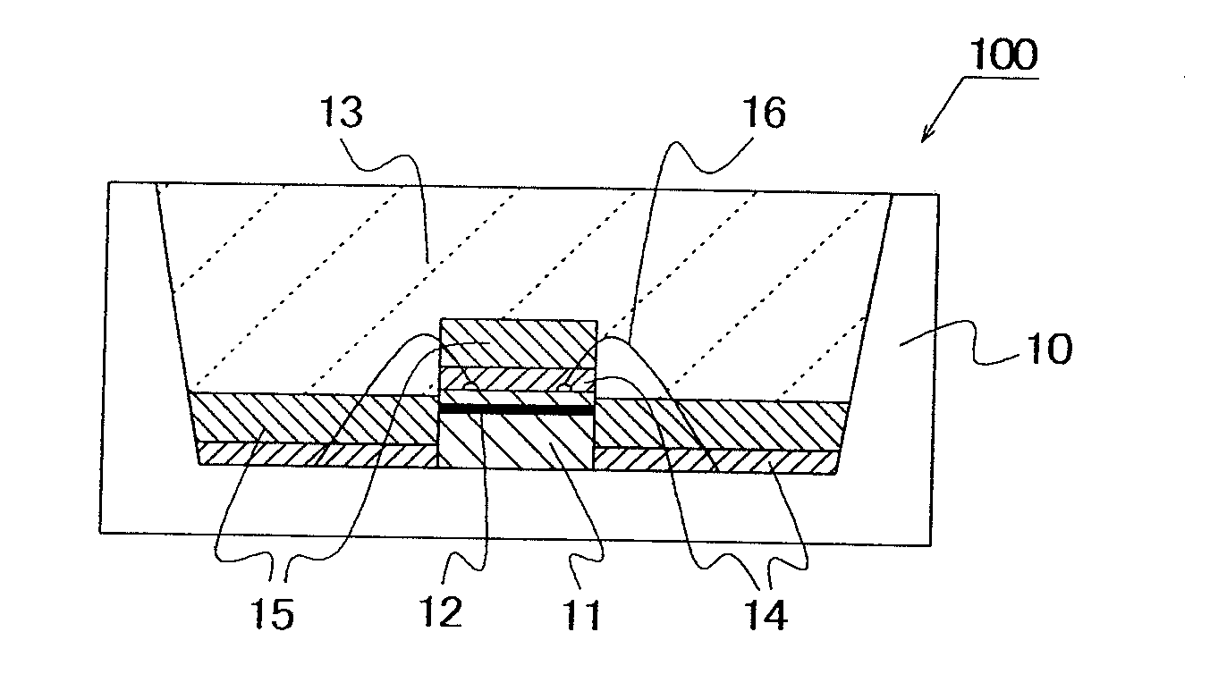
[0055]The light emitting device according to Example 1 will be described with reference to FIG. 1. FIG. 1 is a schematic cross-sectional view of a light emitting device according to the first embodiment of the present invention, and the light emitting device 100 was fabricated as described below.
[0056]The light emitting device 100 according to Example 1 includes a package 10, a light emitting element 11 having a light emitting layer 12, a resin 13, a deposited layer of fluorescent material 14, a deposited layer of filler 15, and wires 16. The resin 13, the fluorescent material particles 21, the inorganic particles 22, and the filler used in Example 1 were as follows.
[0057](1) Resin 13
[0058]Type: Phenyl-containing silicone resin
[0059]Viscosity: 200 to 20000 mPa·s
[0060](2) Fluorescent Material Particle 21
[0061]Composition: Y3Al5O12:Ce
[0062]Specific Gravity: 4.6
[0063]Average Diameter: 10.5 μm
[0064]Median Particle Diameter: 12.5 μm
[0065](3) Inorganic Particle 22
[0066]Type: Colloidal Sil...
PUM
| Property | Measurement | Unit |
|---|---|---|
| Centrifugal force | aaaaa | aaaaa |
| Gravity | aaaaa | aaaaa |
| Fluorescence | aaaaa | aaaaa |
Abstract
Description
Claims
Application Information
 - R&D Engineer
- R&D Manager
- IP Professional
- Industry Leading Data Capabilities
- Powerful AI technology
- Patent DNA Extraction
Browse by: Latest US Patents, China's latest patents, Technical Efficacy Thesaurus, Application Domain, Technology Topic.
© 2024 PatSnap. All rights reserved.Legal|Privacy policy|Modern Slavery Act Transparency Statement|Sitemap