Semiconductor light emitting device

a technology of oxynitride and light-emitting devices, which is applied in the direction of semiconductor devices, luminescent compositions, chemistry apparatuses and processes, etc., can solve the problems of chromaticity variation or “mottling”, poor red color rendition of configuration, and physical and chemical differences in the composition of oxynitride fluorescent materials

Inactive Publication Date: 2007-04-26
KK TOSHIBA
View PDF9 Cites 119 Cited by
  • Summary
  • Abstract
  • Description
  • Claims
  • Application Information

AI Technical Summary

Problems solved by technology

This configuration has a poor red color rendition because of the small amount of red components.
However, the composition of oxynitride fluorescent material is physically and chemically different from that of yellow fluorescent material.
As a result, the two kinds of fluorescent materials are difficult to u...

Method used


Image

  • Semiconductor light emitting device
  • Semiconductor light emitting device
  • Semiconductor light emitting device

Examples


Embodiment Construction

[0026] The embodiment of the invention will now be described with reference to the drawings.

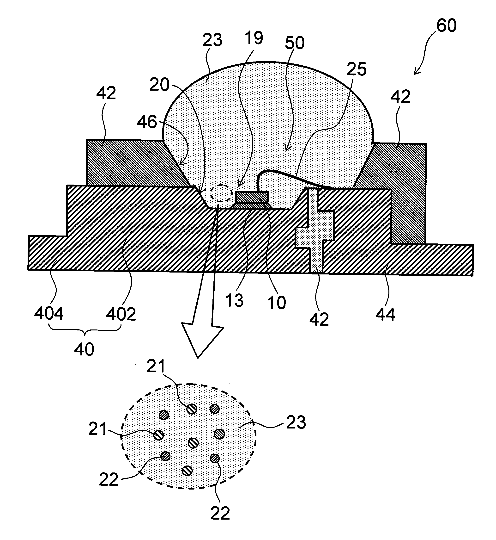
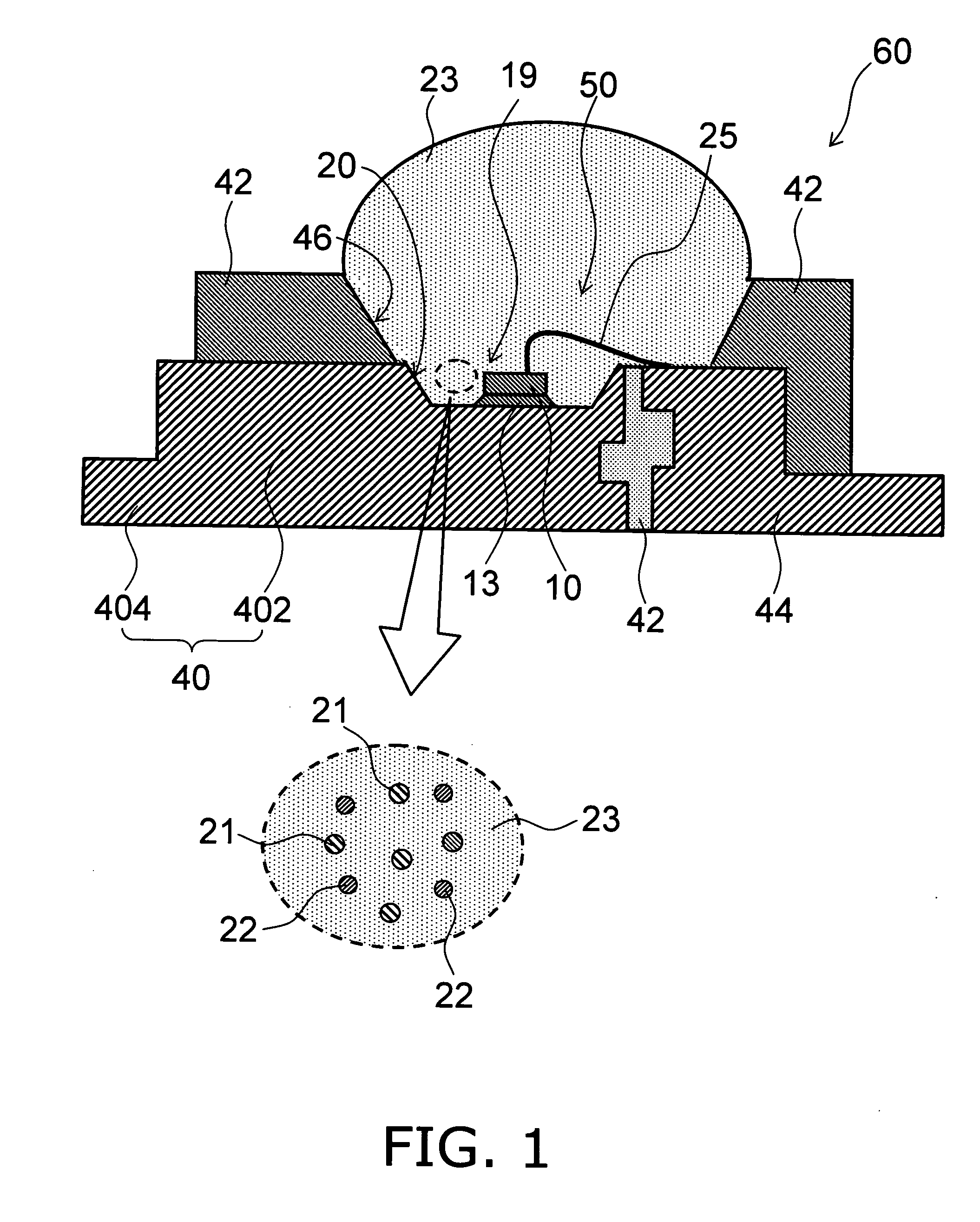
[0027]FIG. 1 is a schematic cross section showing a semiconductor light emitting device 60 according to a first example of the invention.

[0028] The semiconductor light emitting device 60 is configured so that a blue semiconductor light emitting element 10 is bonded with silver paste 13 or the like onto a thick inner lead 402 constituting a first lead 40. The inner lead 402 has a first recess 19, and the semiconductor light emitting element 10 is bonded to the bottom face of the first recess 19.

[0029] An electrode (not shown) provided on the upper face of the semiconductor light emitting element 10 is connected to a second lead 44 via a bonding wire 25. This structure is of the so-called SMD (Surface Mounting Device) semiconductor light emitting device.

[0030] The first lead 40 and the second lead 44, which are made of metal, are buried illustratively in a thermoplastic resin 42. The inner ...


PUM


Abstract

A semiconductor light emitting device comprises: a semiconductor light emitting element that emits first wavelength light; a first fluorescent material that absorbs the first wavelength light and emits second wavelength light having a longer wavelength than the first wavelength light; and a second fluorescent material that absorbs the first wavelength light and emits third wavelength light having a longer wavelength than the second wavelength light. The first fluorescent material and the second fluorescent material are represented by a common chemical composition formula. The first wavelength light, the second wavelength light, and the third wavelength light are combined into light emission of mixed color.

Description

CROSS-REFERENCE TO RELATED APPLICATIONS [0001] This application is based upon and claims the benefit of priority from the prior Japanese Patent Application No. 2005-220549, filed on Jul. 29, 2005; the entire contents of which are incorporated herein by reference. BACKGROUND OF THE INVENTION [0002] In recent years, semiconductor light emitting devices have been widely used in light sources for illumination and display devices. In particular, the realization of blue light emitting elements (blue LED) using gallium nitride (GaN) based materials has dramatically extended the application of white light emitting devices. [0003] A semiconductor light emitting device for white light emission is composed of a gallium nitride based light emitting element having a wavelength range of ultraviolet to blue and fluorescent material that can be excited by absorbing the emitted light to emit light having longer wavelengths. For example, light emission from a blue light emitting element is mixed at a...

Claims


Application Information

Patent Timeline
IPC IPC(8): H01L33/00H01L29/24H01L33/50
CPCC09K11/64C09K11/7734C09K11/7774H01L33/504H01L2224/32257H01L2224/32245H01L2224/48091H01L2224/48247H01L2224/73265C09K11/77342C09K11/77348H01L2924/00014H01L2924/00012H01L2924/00
Inventor OTSUKA, KAZUAKISHIMOMURA, KENJITAKEZAWA, HATSUO
Owner KK TOSHIBA
Why Eureka
Try Eureka